Chongfan Technology
News
20
2026
-
04
New Photonics Approach Achieves On-Chip Light Capture Across a Million Cycles
Author:
For many years, scientists have dreamed of using atomically thin van der Waals materials to fabricate faster, more efficient photonic chips. These materials can be stacked and engineered with extraordinary precision, opening up possibilities far beyond those offered by conventional technologies. However, their extreme fragility has posed a major challenge: standard nanofabrication tools struggle to shape them—a problem that has long been recognized across the field. Now, an international team—including researchers from Aalto University—has broken through this longstanding bottleneck. By developing a technique that can be described as “nanoscale surgery,” they have succeeded in sculpting these delicate materials without causing damage, while achieving record-breaking performance in the process.
This study, published in Nature Materials, marks a significant shift for van der Waals materials—from passive coatings to active building blocks for next-generation photonic and quantum devices.
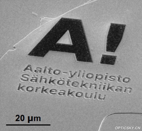
The World’s Thinnest Aalto Logo
Major Challenges in Next-Generation Photonics
Since the rise of graphene, van der Waals materials have captured global attention thanks to their outstanding optoelectronic properties. Their surfaces are atomically smooth and inherently free of dangling bonds, making them highly attractive for photonics—where even minute defects can scatter light and degrade performance. “Despite their enormous potential, using van der Waals materials as structural building blocks has always posed a major challenge,” says Xiaoqi Cui, a researcher at Aalto University. “Standard fabrication methods are far too harsh.” He explains that conventional nanofabrication techniques, such as focused-ion-beam lithography, are often excessively aggressive and can damage the crystal lattice or distort the structures necessary for efficient light trapping.
Solution: Aluminum “Micro-Armor”
To address this challenge, researchers have introduced a concise yet powerful innovation: prior to patterning van der Waals materials, a thin aluminum layer is deposited as a temporary protective shield. “This aluminum layer acts like a miniature armor,” says researcher Andreas Liapis. “It absorbs the damaging impact of the ion beam, enabling us to pattern the material with sub-100-nanometer precision while preserving its crystalline quality.”
A Breakthrough in Quality Factor of One Million
By employing this shielded fabrication approach, the team has created ultra-smooth van der Waals microdisks—miniature circular structures capable of trapping light. These microdisks enable light to circulate repeatedly with extremely low loss, achieving a device quality factor exceeding 1 million, which means that only one part in a million of the optical energy is lost per round trip. In practical applications, light can thus circulate within the microdisk millions of times before experiencing significant attenuation. “This performance represents an improvement of three orders of magnitude over existing van der Waals resonant systems, marking a major breakthrough in this field,” said Professor Zhipeng Sun.
Tenfold improvement in light conversion efficiency
Because light is efficiently confined within the structure, its interaction with the material itself is significantly enhanced, greatly boosting nonlinear optical effects—namely, the conversion of light from one color or frequency to another. When researchers investigated a key nonlinear optical process—second-harmonic generation—they observed an efficiency improvement of four orders of magnitude (i.e., a ten-thousandfold increase) compared with the previous record.
By combining the strong intrinsic nonlinearities of van der Waals materials with ultra-high-quality optical resonances, this study has removed one of the major barriers in the field of van der Waals photonics. This breakthrough opens up new opportunities for reconfigurable photonic circuits, quantum light sources, and highly sensitive on-chip optical sensors. More broadly, it demonstrates that materials once deemed too fragile for fabrication can now be engineered into powerful photonic devices.
Source: phys
Thank you for visiting the official website of Chongfan Technology. If you have cooperation intentions or suggestions, please contact us through the following methods, and we will reply as soon as possible, thank you!
Address: Room 403, Building 6, Phase III of R&D, No. 36 Xiyong Avenue, High tech Zone, Chongqing, China.
Telephone: +86-13658337211
E-mail: Sales@cfkeji.net
Website: www.cfkeji.net
Mobile Version