
Chongfan Technology
News
14
2026
-
08
The Shanghai Institute of Optics and Fine Mechanics has achieved new progress in geometrically induced quantum interference and ultrafast nonlinear optical control in CdO nanograting thin films.
Author:
Recently, the team led by Zhao Yuan’an at the High-Power Laser Components Technology and Engineering Department of the Shanghai Institute of Optics and Fine Mechanics, Chinese Academy of Sciences, in collaboration with the team led by Yao Jianke at South China Normal University, has achieved significant progress in modulating the mid-infrared nonlinear optical properties of cadmium oxide (CdO) nanograting thin films through geometrically induced quantum interference effects. The relevant findings have been published in Optics Express under the title “Mid-Infrared Nonlinear Optical Modulation of CdO Nanogratings Enabled by Geometric Quantum Interference Enhancement.”
Cadmium oxide (CdO) and other epsilon‑near‑zero (ENZ) materials exhibit pronounced nonlinear optical responses in the mid‑infrared spectral region, making them a focal point of cutting‑edge research on photonic devices worldwide. However, these materials typically suffer from limited tunability and modest nonlinear response strengths. To overcome these limitations, the research team designed and fabricated a CdO‑based nanograting structure (CdO‑NG). In this architecture, geometry‑induced quantum interference effects (GQIE) can effectively modulate the material’s Fermi level (EF) and carrier concentration, thereby enabling active control over its mid‑infrared nonlinear optical properties.
Experiments demonstrate that as the grating etching depth increases from 10 nm to 30 nm, the carrier concentration in the CdO nanograting film rises significantly from 8.18 × 10²⁷ cm⁻³ to 43.76 × 10²⁷ cm⁻³, and the Fermi level shifts upward from 2.074 eV to 3.831 eV, enabling geometrically tunable modulation of the electronic band structure over a broad range. At a wavelength of 2 μm (in the ENZ regime), the nonlinear absorption coefficient β increases markedly with both increasing etching depth and incident angle, exhibiting pronounced polarization anisotropy. Specifically, under 60° TM-polarized excitation, the CdO‑NG30 sample achieves a nonlinear absorption coefficient β of −8.63 cm/MW, approximately 1.5 times higher than that of the unstructured CdO thin film (−5.74 cm/MW). Measurements at 3 μm (outside the ENZ regime) further confirm that this anisotropy arises from the intrinsic geometric features of the grating structure. Moreover, carrier dynamics measurements reveal that the structure possesses exceptional ultrafast characteristics, with a transient response time below 220 fs and a modulation bandwidth exceeding 1.6 THz.
This work for the first time introduces geometry‑induced quantum interference effects into the nonlinear control of ENZ materials, enabling broad‑range, structurally tunable modulation of the Fermi level and carrier concentration. The CdO nanograting thin film not only significantly enhances nonlinear absorption in the mid‑infrared regime but also exhibits ultrafast temporal response and broadband modulation capabilities, offering a novel design paradigm for next‑generation ultrafast all‑optical switches, high‑power mid‑infrared photonic devices, and reconfigurable nonlinear optical platforms.
This research was supported by the Chinese Academy of Sciences’ Special Exchange Program, the International Cooperation Bureau’s Key Project on International Collaboration, and Shanghai’s “Explorer” program, among others.
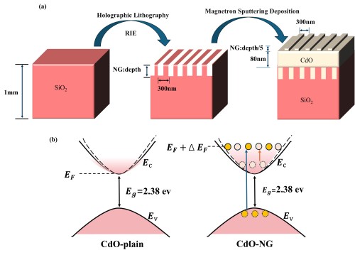
Figure 1. Preparation process and band structures of CdO‑plain and CdO‑NGs. (a) Preparation process of CdO‑NGs; (b) Schematic diagrams of the band structures of CdO‑plain and CdO‑NGs.
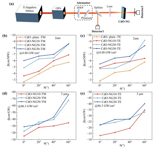
Figure 2. Nonlinear optical characterization of CdO‑plain and CdO‑NGs. (a) Schematic of the open-aperture Z‑scan setup. At a wavelength of 2 μm, the nonlinear absorption coefficient β of CdO‑NGs as a function of incident angle and etching depth: (b) TM polarization; (c) TE polarization. Corresponding variations in the nonlinear absorption coefficient at 3 μm: (d) TM polarization; (e) TE polarization.
Source: Shanghai Institute of Optics and Fine Mechanics
LATEST NEWS
Thank you for visiting the official website of Chongfan Technology. If you have cooperation intentions or suggestions, please contact us through the following methods, and we will reply as soon as possible, thank you!
Address: Room 403, Building 6, Phase III of R&D, No. 36 Xiyong Avenue, High tech Zone, Chongqing, China.
Telephone: +86-13658337211
E-mail: Sales@cfkeji.net
Website: www.cfkeji.net
Mobile Version