
Chongfan Technology
News
17
2026
-
11
Transparent silicon photonic chips could bring advanced optical systems to curved displays.
Author:
In the field of silicon photonics, data is transmitted and processed on semiconductor chips using light instead of electricity, which has driven optical systems to evolve from bulky devices into compact, advanced systems. However, silicon photonic chips are typically rigid and opaque.
Scientists at the Massachusetts Institute of Technology have now developed a scalable method to make silicon photonic chips flexible and transparent, paving the way for advanced microchips that could be used in applications such as discreet health monitors worn on the body or transparent augmented-reality displays tailored to the curved surfaces of pilots’ helmets.
Although scientists have recently demonstrated flexible or transparent chips in the lab, only a small number of devices can be fabricated at a time.
Researchers at MIT worked closely with engineers from NY Creates at the Albany NanoTech Complex to develop a process that uses standard semiconductor manufacturing techniques to produce flexible, transparent silicon photonic chips on large‑size wafers.
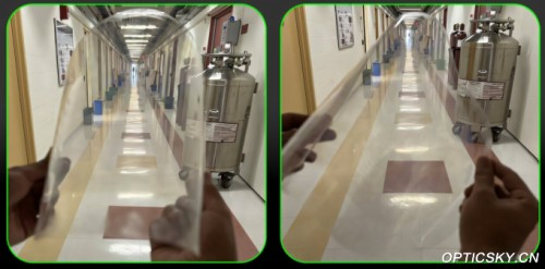
To validate this platform, the researchers bent a single chip around cylinders of varying diameters thousands of times—the thinnest being only as thick as a small screw—without any degradation in performance. They also confirmed that viewing through the chip did not produce noticeable blurring or distortion.
Jelena Notaros, Robert J. Shillman Associate Professor of Electrical Engineering and Computer Science at MIT, a member of the Microsystems Technology Laboratories, and the senior author of the paper on this manufacturing platform, stated: “We have now developed a wafer-scale process that can produce mechanically flexible and optically transparent wafers, enabling new applications previously unattainable in silicon photonics. We hope that, through close collaboration with our colleagues at NY Creates and by leveraging the foundry capabilities of the Albany NanoTech Complex, we can make this platform accessible to other research groups, thereby opening up these new application avenues for the entire field of silicon photonics.” The relevant research findings were published in the journal Optica.
Flexible and transparent
Over the past decade, researchers have developed techniques for the large-scale fabrication of precision, highly reliable silicon photonic devices.
They use advanced microelectronic foundry processes to produce 300-millimeter-diameter wafers containing billions of nanoscale optical devices. However, the silicon photonic chips produced by these methods are rigid and opaque.
Notaros said, “We recognize that many applications would benefit from flexible and transparent chips.”
Scientists have previously fabricated individual transparent or flexible silicon photonic chips, but these techniques could not be scaled. To address this scalability challenge, Notaras’s team recently demonstrated a foundry‑level process for manufacturing silicon photonic chips on flexible substrates.
Now, the team has further advanced these innovations by developing a scalable process capable of producing 300-millimeter silicon photonics wafers that are both transparent and flexible.
Their manufacturing process begins in the same way as that used for conventional rigid silicon wafers. On this rigid silicon substrate, researchers carefully deposit and pattern microscopic light channels known as waveguides.
Then, they bond a temporary silicon wafer to the top. Next, they flip the wafer over and remove the original silicon substrate from the surface that is now on top. What remains is a flat layer of material less than one-tenth the thickness of a human hair.
Sneh said, “Thanks to the rigid temporary support we added before flipping the wafer, we were able to keep thinning it until only the oxide and waveguide layers remained.”
They use an adhesive to bond a thin layer of transparent polyester film to the top of these ultrathin layers, then “debond” and remove the temporary silicon wafer from the bottom.
In this way, they obtained a flexible, transparent wafer only a few micrometers thick, containing the oxide and waveguide layers required for silicon photonics to capture and transmit light.
Sneh added, “Because we are using stable 300-millimeter foundry manufacturing equipment, we can design systems that incorporate a large number of components and be confident that they will meet specification requirements, which is extremely important.”
The greatest challenge in developing this manufacturing process lies in removing enough material from a large 300-millimeter-diameter silicon wafer, leaving behind only a layer just a few micrometers thick.
During manufacturing, stress on the wafer typically causes it to bend slightly, making the process of removing silicon material particularly challenging.
Dyer said, “When we flip the wafers over these substrates, if the strain isn’t properly controlled and the wafer isn’t flat enough, its surface will become rippled, and it may even crack on the production line.”
The researchers carefully controlled this stress by consistently employing low-temperature processes at 500 degrees Celsius or below. They also had to determine the correct sequence and combination of removal methods.
They use industrial processes to thin the silicon layer, but switch to a more precise selective chemical etching step in the final stage. This ensures that the remaining ultra-thin layer remains undamaged.
Focus on performance
The researchers conducted three experiments to test the various functions of these flexible, transparent silicon photonic wafers.
First, they tested the optical performance of chips with integrated waveguides of varying lengths to determine their waveguide characteristics.
They then tested the flexibility by bending the chip around cylinders of varying diameters thousands of times. These experiments showed that performance did not degrade even when bent around a cylinder as thin as a small screw. The device only began to deteriorate after the researchers bent it several times around a toothpick.
Garcia Coleto said, “This experiment has validated that the platform can be used for the applications we proposed, and its performance even exceeds the metrics required by these target systems.”
They also assessed transparency by constructing a bionic eye, testing whether the chip distorted the user’s vision when placed in front of the eye. They found that the chip caused minimal blurring for the observer, and images perceived through it showed no significant distortion.
These characteristics may make such chips particularly well-suited for silicon photonics systems like curved augmented-reality displays—e.g., curved displays integrated into head-up windshields or aircraft pilot visors. Taking the pilot visor as an example, this type of augmented-reality display could replace the bulky optical systems currently used to provide real-time information that helps pilots respond to hazardous situations.
In the future, researchers hope to add more complex components and functionalities to the chip to enable these and other new applications. They also aim to optimize the design to further enhance waveguide efficiency and transparency.
Source: phys
LATEST NEWS
Thank you for visiting the official website of Chongfan Technology. If you have cooperation intentions or suggestions, please contact us through the following methods, and we will reply as soon as possible, thank you!
Address: Room 403, Building 6, Phase III of R&D, No. 36 Xiyong Avenue, High tech Zone, Chongqing, China.
Telephone: +86-13658337211
E-mail: Sales@cfkeji.net
Website: www.cfkeji.net
Mobile Version