
Chongfan Technology
News
05
2026
-
08
New progress has been made in ultra-low-threshold two-dimensional semiconductor lasers.
Author:
Two-dimensional semiconductors have opened up a new pathway toward ultra-low-threshold nanolasers. Recently, the Suzhou Institute of Nano-Tech and Nano-Bionics of the Chinese Academy of Sciences has designed a “twist‑angle photonic crystal nanocavity,” which enables heterostructural integration with monolayer tungsten disulfide by leveraging the cavity’s “air mode.” Under continuous optical pumping at room temperature, the device exhibits stable lasing, setting a new record for the lowest room-temperature threshold among two-dimensional semiconductor lasers.
The team fabricated two finite‑size hexagonal photonic crystals on a single‑layer silicon nitride film and twisted them relative to one another at a chosen angle. This twisting induces a quasi‑continuous radial gradient in the air‑filling fraction of the unit cell, from the center toward the edge, thereby establishing a radially varying bandgap. This graded bandgap can be viewed as a set of finely nested concentric‑ring reflectors that highly confine light fields of specific modes to the central air region, giving rise to an extreme “air‑mode.” In this configuration, the vast majority of the optical field is confined within the air, enabling efficient spatial overlap with excitons in monolayer tungsten disulfide suspended in the air holes. As a result, the excitons emit light with high efficiency in the suspended region, completely circumventing dielectric screening and nonradiative recombination quenching arising at dielectric interfaces.
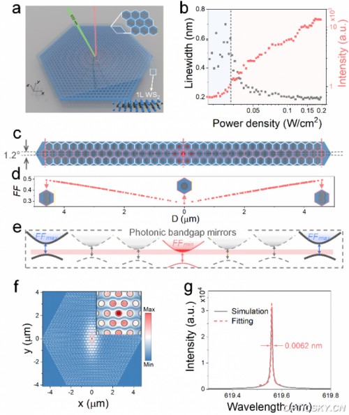
Working principle of two-dimensional semiconductor lasers
This nanocavity achieves an ultracompact mode volume of only 0.36(λ/n)³ and a simulated quality factor as high as 10⁵. Under continuous-wave pumping at room temperature, a monolayer of tungsten disulfide lases at an extremely low power density of 0.03 W/cm², setting a new record for the threshold of two-dimensional semiconductor lasers and paving a completely new path for the development of ultra‑low‑power on‑chip light sources.
The relevant research findings have been published in Advanced Materials. This work was supported by the National Key R&D Program, the National Natural Science Foundation of China, and other funding sources.
Source: Suzhou Institute of Nanotechnology and Nano-Bionics
LATEST NEWS
Thank you for visiting the official website of Chongfan Technology. If you have cooperation intentions or suggestions, please contact us through the following methods, and we will reply as soon as possible, thank you!
Address: Room 403, Building 6, Phase III of R&D, No. 36 Xiyong Avenue, High tech Zone, Chongqing, China.
Telephone: +86-13658337211
E-mail: Sales@cfkeji.net
Website: www.cfkeji.net
Mobile Version