
Chongfan Technology
News
05
2026
-
08
Huazhong University of Science and Technology has achieved a significant breakthrough in the field of programmable optical processing chips.
Author:
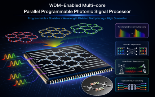
Recently, a research team led by Professor Minming Zhang and Associate Professor Shuang Zheng from the School of Optoelectronic Information at Huazhong University of Science and Technology and the Wuhan National Laboratory for Optoelectronics, in collaboration with Professor José Capmany of the Polytechnic University of Valencia in Spain, has proposed a wavelength-division-multiplexing–enabled multi-core parallel programmable photonic processor (Optical Field-Programmable Photonic Arrays, OFPPA). This work is the first to introduce the wavelength dimension into a two-dimensional programmable optical network architecture, significantly enhancing the functional density and computational power of programmable photonic processors. The related research findings have been published in Nature Communications under the title “WDM-enabled multi-core parallel programmable photonic signal processor.”
In fields such as artificial intelligence, large-scale data centers, and high-speed optical communications, traditional electronic processors are approaching physical limits in clock speed, thermal dissipation, and bandwidth. Programmable photonic processors, leveraging the high‑speed, low‑latency characteristics of photons, emerge as a promising key solution. Analogous to electrical field-programmable gate arrays (FPGAs), optical field‑programmable photonic arrays (OFPPAs) can dynamically reconfigure a single photonic hardware platform to implement diverse optical signal‑processing functions, significantly reducing the development cycle and fabrication costs of dedicated photonic integrated circuits. In recent years, research teams worldwide have been working to develop larger‑scale programmable array chips capable of supporting more advanced optical signal processing tasks, including optical computing, optical switching, optical routing, and WDM filtering. However, existing chip designs typically rely on a programmable optical mesh architecture based on tunable Mach–Zehnder interferometers, in which all wavelength channels share the same network configuration. This makes independent wavelength‑level configuration difficult, severely constraining the parallel processing capabilities of photonic chips.
In response to the aforementioned challenges, the research team proposed a MRR–MZI composite architecture as the fundamental building block. By integrating over‑coupled thermo‑optic tunable microring resonators into both arms of the MZI, they achieved synergistic multiplexing across spatial and wavelength dimensions within a hexagonal two‑dimensional reconfigurable network. The introduction of wavelength‑division multiplexing enables a single physical chip to simultaneously construct distinct photonic networks at different wavelengths, substantially enhancing its parallel processing capacity. Experimental results demonstrate an expanded free spectral range of 8 nm (1 THz) and a reduced tuning power consumption of 4.3 mW/π—improvements nearly an order of magnitude compared with conventional MZI units—while achieving a device functional density of 169.6/mm².
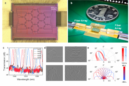
The research team validated the architecture’s versatility through three representative applications: configuring it as a tunable band‑notch filter to achieve an extinction ratio exceeding 30 dB; performing entirely distinct matrix operations on two different wavelengths simultaneously within the same physical grid; and constructing a dual‑beam, tunable optical delay network to realize microwave photonic dual‑beamforming. The experimental results fully demonstrate the chip architecture’s multifunctional parallel‑processing capabilities, paving the way for on‑chip programmable optical processing systems in areas such as optical communications, photonic computing, and radar signal processing.
It is reported that the teams led by Zhang Minming and Zheng Shuang have long been dedicated to research in areas such as optoelectronic‑integrated chips for computing‑power interconnects, silicon‑based heterogeneous integration technologies, and intelligent chip design. They have undertaken a series of major national key projects and research topics, and have published a number of significant findings in high‑impact journals—including Nature Communications and Light: Science & Applications—and at international conferences.
Yang Zihang and Li Yunlong, graduate students at Huazhong University of Science and Technology, are the co-first authors of the paper, while Zhang Minming, Zheng Shuang, Shen Li, and Professor José Capmany serve as the co-corresponding authors. Huazhong University of Science and Technology is the primary institution responsible for the research. This work also benefited from the guidance and support of Professor Wim Bogaerts of Ghent University in Belgium, a leading expert in silicon photonics.
Source: Huazhong University of Science and Technology
LATEST NEWS
Thank you for visiting the official website of Chongfan Technology. If you have cooperation intentions or suggestions, please contact us through the following methods, and we will reply as soon as possible, thank you!
Address: Room 403, Building 6, Phase III of R&D, No. 36 Xiyong Avenue, High tech Zone, Chongqing, China.
Telephone: +86-13658337211
E-mail: Sales@cfkeji.net
Website: www.cfkeji.net
Mobile Version