
Chongfan Technology
News
24
2026
-
07
Chinese scientists have created a brand-new topological photonic “highway.”
Author:
Recently, Professor Cui Xiaohan of the Electromagnetic Metamaterials Team at Southeast University’s National Key Laboratory of Millimeter Waves, together with Associate Professor Zhang Ruoyang of Nanjing University and the team of Professor Chen Ziting at the Hong Kong University of Science and Technology, have proposed and demonstrated a novel topological photonic waveguide—a topology‑protected, insulator‑free, multi‑channel “highway” for light. The findings have been published in the internationally renowned journal Nature. This work addresses the longstanding challenge in conventional topological photonic waveguides—balancing topological protection with spatial efficiency—by offering a new approach to this problem.
As optical communication and photonic computing continue to advance, the challenge of packing more channels into a limited footprint while minimizing reflection and crosstalk has become a central issue in integrated photonics. Although topological waveguides can guide light around defects and sharp bends, they require relatively wide photonic insulator regions to provide topological protection and confine the optical field; these regions do not contribute to signal transmission, thereby limiting the spatial efficiency of the device.
One can think of conventional topological waveguides as dedicated roads enclosed by broad, insulating barriers: vehicles travel stably, yet the usable roadway occupies only a small fraction of the total space. By contrast, the “photonic highway” constructed in this study resembles a densely packed, multi‑lane freeway—where each channel not only carries its own signal but also serves as a “guardrail” for adjacent channels, thereby eliminating the need for extensive additional isolation layers.
The underlying physical principle is a set of four specialized photonic crystals—photonic valley semimetals—designed by the team. One of their two band‑valley degrees of freedom manifests as a Dirac semimetal with no band gap, while the other behaves as a topological insulator, enabling it to serve simultaneously as both a waveguide and a topological photonic insulating layer. By arranging these four valley semimetals in a specific sequence, one can construct four spatially parallel unidirectional channels. These distinct channels cooperate to ensure topological unidirectional transmission in each region while achieving 100% spatial utilization.
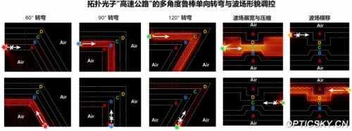
The team constructed an experimental platform in the microwave frequency range, demonstrating four unidirectional waveguide channels and showing that electromagnetic waves can propagate unidirectionally along the designated paths even when subjected to sharp bends of 60°, 90°, and 120°, with backscattering and inter-channel crosstalk effectively suppressed. Unlike conventional topological waveguides, where light is predominantly confined near narrow interfaces, the waves in this new structure can be distributed throughout the entire channel. Consequently, by adjusting the channel’s width and geometry, it is possible to broaden, compress, or laterally shift the field distribution, opening up new possibilities for simultaneously achieving signal transmission and wave‑field shaping within compact spaces.
This achievement breaks through the conventional paradigm in fundamental research, which has long relied on material boundaries or interfaces for topological light transmission, and opens up a new pathway for parallel, unidirectional, robust light guiding across the entire device area. At the application level, it holds promise as a novel solution for high‑density photonic chips, reducing wasted space while increasing channel density and information‑carrying capacity. According to the team, this technology could eventually be extended to multiple practical frequency bands, including optical communications and terahertz regimes. However, to achieve real‑world deployment, several engineering challenges must still be addressed, such as material losses, device coupling, and integration with functional components of photonic chips.
This cross‑institutional collaborative breakthrough represents a significant original advance in China’s fields of topological photonics and integrated photonics, offering a novel underlying physical framework that simultaneously addresses “stable transmission” and “high‑density integration,” while also laying the theoretical and technological groundwork for independent innovation in next‑generation high‑speed optical communications and on‑chip photonic computing.
Chen Ziting is the corresponding author of the paper, while Cui Xiaohan and Zhang Ruoyang are the co-first authors and co-corresponding authors, respectively.
Source: Southeast University
LATEST NEWS
Thank you for visiting the official website of Chongfan Technology. If you have cooperation intentions or suggestions, please contact us through the following methods, and we will reply as soon as possible, thank you!
Address: Room 403, Building 6, Phase III of R&D, No. 36 Xiyong Avenue, High tech Zone, Chongqing, China.
Telephone: +86-13658337211
E-mail: Sales@cfkeji.net
Website: www.cfkeji.net
Mobile Version