
Chongfan Technology
News
28
2026
-
05
Two-dimensional material WS₂, valley–spin electronic chip | Nature Photonics
Author:
Transition-metal dichalcogenides, as direct‑bandgap semiconductors, exhibit a strong coupling between valley degrees of freedom and valley‑polarized excitons excited by circularly polarized light, enabling valley‑dependent chiral photonics and, consequently, ultrafast optically driven valleytronics. However, achieving fully integrated valley photonics—namely, on‑chip in situ generation, selective routing, and electrical readout of valley‑dependent chiral photons—remains one of the most challenging open problems.
Recently, a team led by Ren Haoran and Stefan A. Maier at Monash University in Australia, in collaboration with Professor Dong Zhaogang of Singapore’s Agency for Science, Technology and Research and Professor Ou Qingdong of the Macau University of Science and Technology, published an article in Nature Photonics reporting a valley‑driven hybrid optoelectronic nanocircuit that integrates chiral‑selective superwaveguide photodetectors with transition‑metal dichalcogenides.
At room temperature, the specially designed hyper‑waveguide device, encapsulating a monolayer of tungsten disulfide, generates nearly perfect valley‑dependent chiral photons—exhibiting a chirality close to unity—during second‑harmonic generation. These photons are selectively coupled into unidirectional waveguide modes, achieving polarization selectivity as high as 0.97. The resulting valley‑dependent waveguide modes are detected by an atomically thin, few‑layer tungsten diselenide photodetector that responds only to up‑converted photons above the bandgap, thereby enabling on‑chip processing of valley‑multiplexed images.
This work bridges a critical gap in valleytronics, paving the way for compact, programmable, and scalable valley‑information processing and advancing the development of photonics‑based valleytronic quantum technologies.

First authors: Chi Li (Li Chi), Kaijian Xing (Xing Kaijian) Corresponding authors: Qingdong Ou (Ou Qingdong), Zhaogang Dong, Stefan A. Maier & Haoran Ren Affiliations: Monash University, Agency for Science, Technology and Research (A*STAR), Macau University of Science and Technology An on-chip programmable valley optoelectronic nanocircuit. On-chip programmable valley optoelectronic nanocircuit
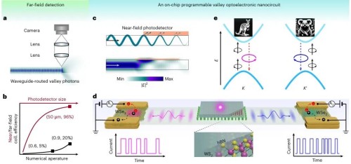
Figure 1 | Schematic of the waveguide‑based photonic detection scheme and the on‑chip programmable valley‑photonic nanocircuit, illustrating the differences in collection efficiency between far‑field and near‑field detection, and elucidating the operating principles of all‑on‑chip valley‑dependent chiral photon generation, selective routing, and electrical detection, along with the band diagram governing the nonlinear valley‑selection rules.
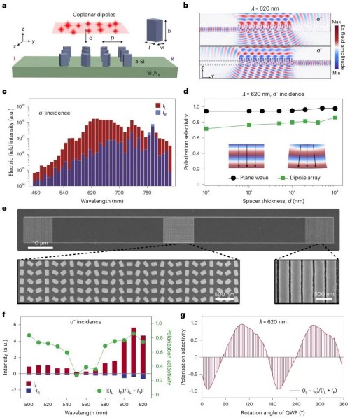
Figure 2 | Design, simulation, and experimental characterization of a chiral‑selective metamaterial waveguide, including its three‑dimensional configuration, electric field distribution, wavelength‑dependent coupling strength, the dependence of polarization selectivity on interlayer spacing, as well as SEM images of the fabricated sample and the results of far‑field experiments on the selective routing of circularly polarized light.
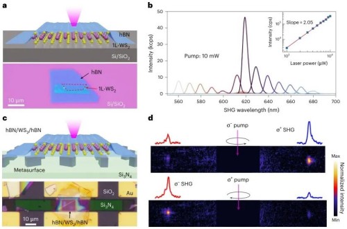
Figure 3 | Generation of valley‑dependent chiral photons and unidirectional waveguide routing, showing the second-harmonic generation characteristics of hBN‑encapsulated monolayer WS₂, their wavelength and power dependencies, as well as far-field optical images demonstrating unidirectional routing of SHG photons via an metasurface waveguide.
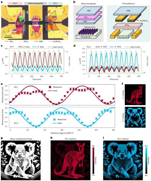
Figure 4 | Characterization of the VMP device integrated with a WSe₂ photodetector and demonstration of valley multiplexing for image processing, including device architecture, photocurrent response, polarization sensitivity measurements, as well as valley‑encoding input and photodetector‑decoded output for Kangaroo and Koala images.
Source: Today’s New Materials
LATEST NEWS
Thank you for visiting the official website of Chongfan Technology. If you have cooperation intentions or suggestions, please contact us through the following methods, and we will reply as soon as possible, thank you!
Address: Room 403, Building 6, Phase III of R&D, No. 36 Xiyong Avenue, High tech Zone, Chongqing, China.
Telephone: +86-13658337211
E-mail: Sales@cfkeji.net
Website: www.cfkeji.net
Mobile Version