Chongfan Technology
News
11
2026
-
05
Shanghai Institute of Optics and Fine Mechanics Achieves Progress in Research on Ion-Sliced Nd:YAG Laser Ceramics and On-Chip Amplifiers
Author:
Recently, a research team led by Researcher Jun Wang from the Department of Frontier Interdisciplinary Photonics at the Shanghai Institute of Optics and Fine Mechanics, Chinese Academy of Sciences, has made progress in the study of ion-sliced Nd:YAG laser ceramics and their on-chip amplifiers. The relevant research findings have been published in Materials & Design under the title “Ion slicing of Nd:YAG Laser ceramics on sapphire platform and its waveguide amplifier design at 1064 nm.”
The fabrication of sub-micron solid-state laser gain films is a critical pathway for achieving high-power on-chip optical amplification, and combining bulk materials doped with rare-earth gain ions with SmartCut (ion milling or ion slicing) technology holds promise for breakthroughs in film performance. The research team has, for the first time, applied ion slicing to Nd:YAG laser ceramics, systematically elucidating the dual mechanisms by which grain boundaries contribute to stress relaxation during annealing. Experimental results show that in the low-temperature range of 550–850 °C, helium ions accumulate along grain boundaries, forming bubbles that trigger grain collapse; above 850 °C, helium atoms acquire sufficient kinetic energy to traverse grain boundaries, thereby triggering the cohesive delamination of the entire film layer. Based on these findings, a gradient annealing strategy—pre-annealing at 400 °C followed by rapid annealing at 900 °C—is proposed. This approach uses the pre-annealing stage to preemptively relieve the internal stresses that drive grain collapse, thus allowing cohesive delamination to become the dominant mechanism during the high-temperature phase. Using this strategy, the researchers successfully achieved controlled transfer of a 915-nm-thick ceramic film, several hundred micrometers wide laterally, onto a sapphire substrate.
Researchers further conducted a systematic characterization of the transferred thin film using transmission electron microscopy (TEM), atomic force microscopy (AFM), and photoluminescence (PL) spectroscopy. TEM images revealed a sharp and well-defined interface between the thin film and the substrate, with no dislocations or amorphous phases introduced; AFM measurements indicated a surface roughness of approximately 2.5 nm; and PL spectroscopy confirmed that the main emission peak at 1064 nm and its intensity are in excellent agreement with those of the bulk ceramic, thereby fully demonstrating the non-destructive nature of the ion-slicing process and its feasibility for device fabrication.
Based on this Nd:YAG ceramic–sapphire heterogeneous integration platform, the team designed and optimized the Si3N4 waveguide amplifier structure. Finite-element simulations were used to tune the waveguide width, height, and gain-layer thickness, resulting in confinement factors of 35.16% for the 808 nm pump light and 38.51% for the 1064 nm signal light in the TM mode. Simulation results indicate that, with a waveguide length of 12 cm and a pump power of 160 mW, the device can achieve a peak internal gain of approximately 25 dB at 1064 nm.
This work for the first time validates the feasibility of fabricating ceramic gain films using ion-slicing technology and elucidates a dual-path mechanism of grain-boundary–mediated stress relaxation, thereby offering a new technological route for on-chip integration of laser ceramic materials and the design of high-performance waveguide amplifiers.
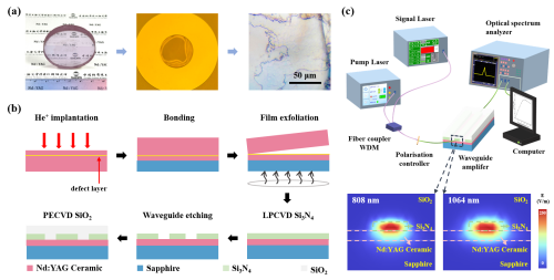
Figure 1: Process flow and subsequent device testing diagrams: (a) Nd:YAG ceramic film delamination process; (b) Device fabrication process flowchart; (c) Schematic diagram of the optical gain measurement setup.
Source: Shanghai Institute of Optics and Fine Mechanics
Thank you for visiting the official website of Chongfan Technology. If you have cooperation intentions or suggestions, please contact us through the following methods, and we will reply as soon as possible, thank you!
Address: Room 403, Building 6, Phase III of R&D, No. 36 Xiyong Avenue, High tech Zone, Chongqing, China.
Telephone: +86-13658337211
E-mail: Sales@cfkeji.net
Website: www.cfkeji.net
Mobile Version