Chongfan Technology
News
09
2026
-
03
Magneto‑electric/Spintronic Materials – On‑Chip Integrated Microwaves
Author:
Microwave technology plays a crucial role in fields such as communications, physics, and medicine. At present, microwave antennas, detectors, and other components are continuously evolving toward miniaturization, integration, and intelligentization. However, traditional microwave detection systems typically consist of antennas, filters, amplifiers, and rectifying circuits, resulting in relatively large overall sizes. The system’s bulkiness and high power consumption severely limit further integration and broader application expansion.
Recently, the Nanofabrication Platform at the Suzhou Institute of Nano-Tech and Nano-Bionics, Chinese Academy of Sciences, together with its collaborating teams, has made significant progress in the research on on-chip integrated microwave devices, successfully achieving, for the first time, monolithic integration of magnetoelectric antennas with nanoscale spin detectors. The related research findings, titled “A CMOS‑compatible, scalable and compact magnetoelectric spin‑torque microwave detector,” were published online in Nature Nanotechnology (https://www.nature.com/articles/s41565-026-02129-w).
First author: Shuhui Liu, Riccardo Tomasello. Corresponding authors: Bin Fang, Giovanni Finocchio & Zhongming Zeng. Affiliations: Suzhou Institute of Nano-Tech and Nano-Bionics, Chinese Academy of Sciences; University of Messina, Italy.
The research team innovatively proposed a monolithic integration strategy for magnetoelectric and spintronic materials. By employing magnetron sputtering and chemical mechanical polishing, they achieved atomic‑level precision in the monolithic integration of multiple materials. Further integrating micro‑ and nano‑fabrication with MEMS processing techniques, they fabricated on‑chip integrated devices compatible with CMOS processes. These devices have a total area of less than 0.4 mm² and enable highly sensitive wireless detection of microwave signals, with a detection sensitivity exceeding 90 kV/W and a noise equivalent power as low as approximately 3 pW/√Hz.
This work builds upon the team’s previous achievements (Nat. Commun. 7, 11259, 2016; Phys. Rev. Appl. 11, 014022, 2019; Appl. Phys. Lett. 121, 203504, 2022; Nat. Commun. 14, 2183, 2023). The integrated technology boasts excellent scalability; the research team has successfully fabricated a scalable on-chip microwave detection array, with sensitivity further enhanced to 446 kV/W, laying a solid foundation for subsequent technological transfer and practical applications.
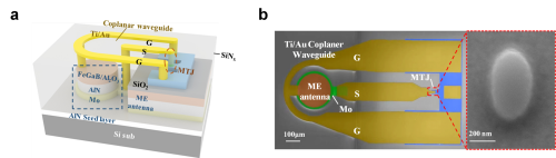
Figure 1: Device Structure and Scanning Electron Micrograph of an On-Chip Integrated Microwave Detector
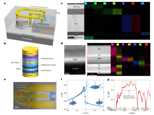
Figure 1 | Device Structure and Characteristics.
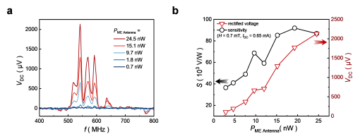
Figure 2: Microwave Response Characteristics of On-Chip Integrated Microwave Detectors
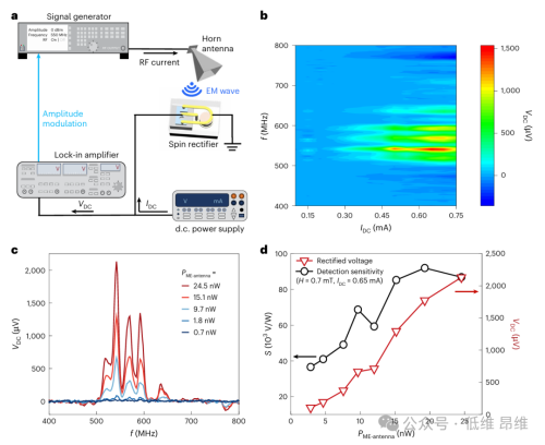
Figure 2 | Wireless Detection Performance of the Device
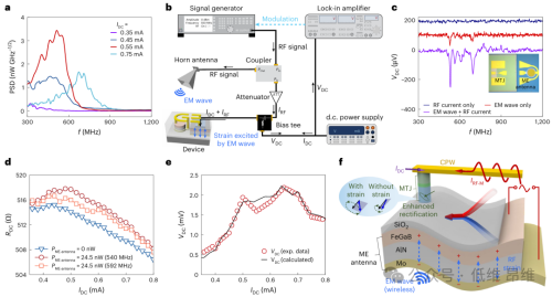
Figure 3 | Working principle of a magnetoelectric spin-torque microwave detector.
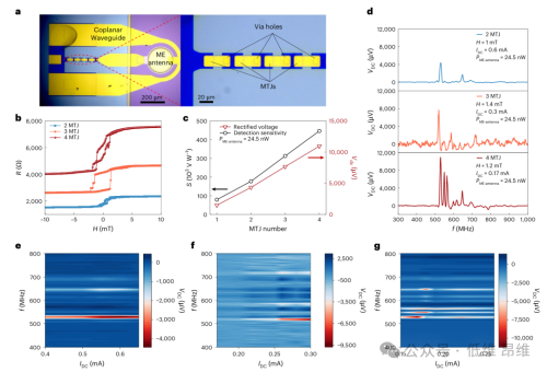
Figure 4 | Detection performance of series-connected multi-magnetic tunnel junction devices.
This research has achieved a significant breakthrough in monolithic integration technology, laying the process and device foundations for the development of a new generation of miniaturized microwave detectors that are highly sensitive and scalable. The Suzhou Institute of Nano-Tech and Nano-Bionics, Chinese Academy of Sciences, served as the primary completing institution. Liu Shuhui, a doctoral candidate at the Suzhou Institute of Nano-Tech and Nano-Bionics, and Associate Professor Riccardo Tomasello of the Polytechnic University of Bari in Italy, are co-first authors; Project Researcher Fang Bin of the Suzhou Institute of Nano-Tech and Nano-Bionics, Professor Giovanni Finocchio of the University of Messina in Italy, and Researcher Zeng Zhongming of the Suzhou Institute of Nano-Tech and Nano-Bionics are co-corresponding authors. The study also benefited from the guidance and support of experts including Professor Zhang Xixiang of King Abdullah University of Science and Technology in Saudi Arabia, Professor Chen Aitian of the University of Electronic Science and Technology of China, and Associate Professor Zhang Likke of Wuxi Institute. This work was funded by projects such as the National Natural Science Foundation of China, the Young Scientists Program under the Key R&D Plan, the Jiangsu Province Frontier Project, the Chinese Academy of Sciences’ Pioneer Action Talent Recruitment Program, and the Suzhou Gusu Leading Talents Program.
Source: Suzhou Institute of Nano-Tech and Nano-Bionics
LATEST NEWS
Thank you for visiting the official website of Chongfan Technology. If you have cooperation intentions or suggestions, please contact us through the following methods, and we will reply as soon as possible, thank you!
Address: Room 403, Building 6, Phase III of R&D, No. 36 Xiyong Avenue, High tech Zone, Chongqing, China.
Telephone: +86-13658337211
E-mail: Sales@cfkeji.net
Website: www.cfkeji.net
Mobile Version