Chongfan Technology
News
27
2026
-
02
The Shanghai Institute of Optics and Mechanics has achieved new progress in enhancing the optoelectronic properties of boron-doped diamond.
Author:
Recently, the Laser Crystal Research Center of the Advanced Laser and Optoelectronic Functional Materials Division at the Shanghai Institute of Optics and Fine Mechanics, Chinese Academy of Sciences, in collaboration with the School of Electronic Science and Engineering at Nanjing University and Zhejiang Infinite Drill Technology Development Co., Ltd., has achieved new progress in enhancing the optoelectronic properties of boron-doped diamond. The related research findings, titled “Optical and electrical properties of CVD boron-doped diamond following HPHT annealing,” have been published in Diamond and Related Materials.
Boron-doped diamond (BDD), owing to its outstanding performance, is regarded as a semiconductor material with great potential. However, achieving efficient p-type conductivity remains challenging: at low boron doping concentrations, the relatively deep acceptor levels result in low activation efficiency, thereby limiting the carrier concentration at room temperature; while heavy doping leads to impurity scattering and defect formation, which in turn reduce mobility.
The research team grew diamond films with varying boron doping concentrations using microwave plasma chemical vapor deposition (MPCVD). These films were then subjected to high-temperature and high-pressure annealing at pressures ranging from 5 GPa and temperatures between 1100 and 2000 °C, allowing for a systematic investigation of the changes in their optical and electrical properties. The experimental results showed that, under appropriate conditions, high-temperature and high-pressure annealing can increase the carrier concentration in B-doped diamond (BDD) by more than one order of magnitude and boost the electrical conductivity by more than four times. The extent of these effects strongly depends on both the annealing temperature and the doping concentration. Comprehensive spectral analysis revealed several factors responsible for the temperature-dependent behavior of carrier concentration during annealing, including lattice strain relaxation, modification of boron-bound excitons, and transformation of nitrogen-vacancy centers. Moreover, the optimal annealing temperature varies significantly with the doping concentration. These findings suggest that high-temperature and high-pressure treatment represents a viable approach to overcoming doping limitations in BDD, thereby paving the way for its broader application in electronic devices.
This work was supported by the National Natural Science Foundation of China.
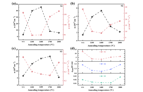
Figure 1: Relationship between the room-temperature carrier concentration, mobility, and Hall resistivity of BDD samples with different boron doping concentrations as a function of annealing temperature.
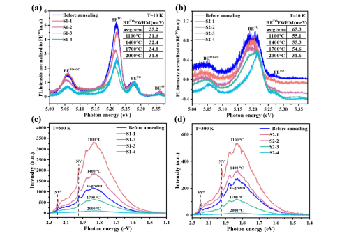
Figure 2. BDD samples annealed at different temperatures: (a) Photoluminescence spectra excited at 213 nm at low temperature (10 K); (b) Photoluminescence spectra excited at 532 nm at room temperature (300 K).
Source: Shanghai Institute of Optics and Fine Mechanics
LATEST NEWS
Thank you for visiting the official website of Chongfan Technology. If you have cooperation intentions or suggestions, please contact us through the following methods, and we will reply as soon as possible, thank you!
Address: Room 403, Building 6, Phase III of R&D, No. 36 Xiyong Avenue, High tech Zone, Chongqing, China.
Telephone: +86-13658337211
E-mail: Sales@cfkeji.net
Website: www.cfkeji.net
Mobile Version