
Chongfan Technology
News
08
2026
-
07
Photonic Crystals | Nature Nanotechnology
Author:
At the nanoscale, electrically injecting charge carriers into photonic structures remains a fundamental challenge, as the conductive pathways required for electrical control can disrupt the optical environment necessary for strong light–matter interactions.
Recently, the research team led by Professor Boubacar Kanté at the University of California, Berkeley, published a paper in Nature Nanotechnology reporting a monolithic nanophotonic architecture that, for the first time, achieves direct electrical injection into extended photonic modes within a single crystal‑cell layer, while fully preserving the maximal refractive index contrast between the semiconductor and air and maintaining the symmetry of the optical cavity.
A quasi‑suspended photonic crystal aperture is employed: it is supported by an array of subwavelength InP nanocolumns strategically positioned at the electromagnetic field nodes of a continuous‑domain bound state (BIC) mode. This configuration enables uniform hole injection across hundreds of unit cells while preserving the optical modes, and simultaneously serves as a thermal‑dissipation pathway.
The study reveals that the transition from single-point injection to distributed injection gives rise to new mechanisms, in which the uniformity of electrical properties—rather than optical properties—emerges as the primary constraint. Consequently, precise control over the uniformity of nanocolumns is essential for achieving lasing. Electrical-pumping lasing at room temperature and at telecom wavelengths demonstrates the feasibility of this architecture. These findings establish a general framework for decoupling electron transport from nanophotonic mode engineering.
Monolithic manufacturing of an electrically addressable quasi-suspended nanophotonic aperture. Monolithic fabrication of an electrically addressable quasi-suspended nanophotonic aperture.
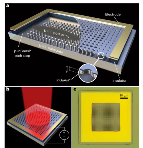
Figure 1. Electrically addressable quasi‑free‑space nanophotonic aperture.
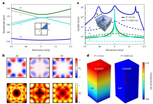
Figure 2. Optical and thermal design of the quasi‑free‑standing photonic crystal.
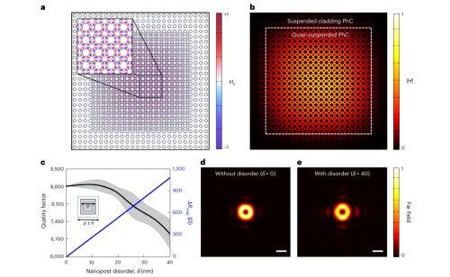
Figure 3. Design of a quasi‑free‑standing photonic crystal cavity and the impact of disordered nanocolumns on its optical and electrical properties.
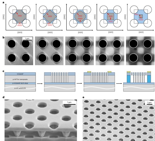
Figure 4. Formation mechanism of the nanopillar array and monolithic device fabrication.
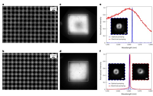
Figure 5. Experimental evidence for the critical role of uniform nanopillar fabrication.
Source: Today’s New Materials
LATEST NEWS
Thank you for visiting the official website of Chongfan Technology. If you have cooperation intentions or suggestions, please contact us through the following methods, and we will reply as soon as possible, thank you!
Address: Room 403, Building 6, Phase III of R&D, No. 36 Xiyong Avenue, High tech Zone, Chongqing, China.
Telephone: +86-13658337211
E-mail: Sales@cfkeji.net
Website: www.cfkeji.net
Mobile Version