
Chongfan Technology
News
06
2026
-
07
The Shanghai Institute of Optics and Fine Mechanics has made progress in research on grating inverse design and closed-loop process optimization.
Author:
Recently, the research team led by Shao Jianda and Jin Yunxia at the High-Power Laser Components Technology and Engineering Department of the Shanghai Institute of Optics and Fine Mechanics, Chinese Academy of Sciences, has made progress in their study on ensemble-learning–assisted inverse design and closed-loop process optimization for spectral-dispersion gratings used for beam smoothing. The relevant findings, titled “Ensemble learning-assisted inverse design and closed-loop process optimization for smoothing by spectral dispersion gratings,” have been published in Advanced Photonics Nexus.
Spectral Dispersion Smoothing (SSD) gratings are the core components of beam‑smoothing systems in large‑scale, high‑power laser facilities such as inertial confinement fusion devices. Their performance directly determines the uniformity of irradiation on the target surface and the effectiveness of suppressing instabilities in laser–plasma interactions. Consequently, achieving high and balanced diffraction efficiency across a broad spectral range and for multiple polarization states is the primary goal in fabricating these gratings. However, the fabrication of high‑performance SSD gratings presents an extremely complex technological challenge. Their optical performance is governed by a multitude of subwavelength‑scale structural parameters, including groove depth and duty cycle, which exhibit strong nonlinear couplings and are highly sensitive to process variations. Traditional trial‑and‑error or empirically driven process‑development approaches are not only time‑consuming and costly but also struggle to precisely optimize the concurrent performance for both polarization states under intricate parameter conditions.
In response to the aforementioned challenges, the research team has proposed a closed-loop optimization framework for SSD grating fabrication, grounded in ensemble-learning–based inverse design and physics‑interpretable validation. By constructing a weighted‑average ensemble learning model (WA‑ELM), they achieved high‑accuracy predictions of the four key structural parameters of SSD gratings. Furthermore, by systematically comparing the correlation between model predictions and experimental measurements, the team demonstrated that WA‑ELM incorporates genuine physical principles underlying the fabrication process, rather than merely performing numerical fitting, thereby substantially enhancing both the model’s reliability and interpretability.
More importantly, the research team has achieved a paradigm shift in process development by establishing a clear mapping chain that links target optical performance to predicted structural parameters and implementable process parameters. In this framework, structural parameters serve as a pivotal physical bridge, transforming the traditional black-box trial-and-error approach into a goal‑oriented design process. The trained WA‑ELM model functions as an efficient process compiler: when presented with specified performance targets, it can generate a process recipe within milliseconds, eliminating the need for time‑consuming iterative cycles. This capability was ultimately validated through fabrication experiments, successfully closing the performance loop from design to physical realization. This method offers a high‑precision, highly reliable solution for the intelligent, customizable fabrication of SSD gratings and other high‑performance micro‑ and nano‑optical components.

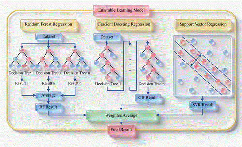
Figure 1. Schematic diagram of the proposed ensemble learning model framework.
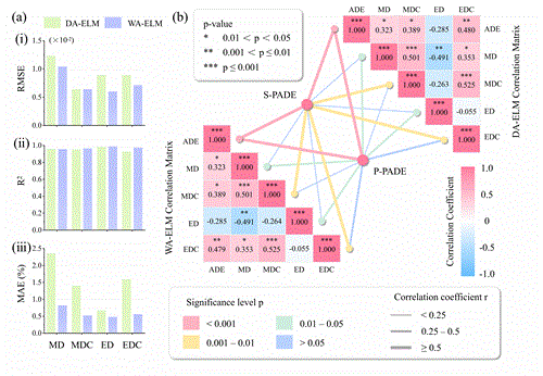
Figure 2: Performance comparison, correlation analysis, and prediction results of two ensemble models. (a) Evaluation metrics for four key structural parameters obtained by DA-ELM and WA-ELM. (b) Correlation matrix of the predicted values from the two ensemble learning models.
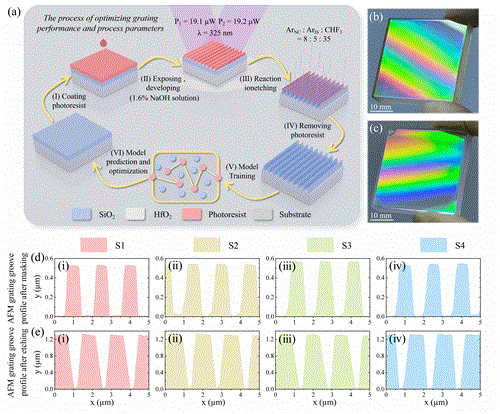
Figure 3 Closed-loop process validation and experimental results based on the ensemble model: (a) Detailed workflow for optimizing the SSD grating fabrication process; (b) Physical images of the mask and (c) the sample after etching; (d) The mask and (e) the AFM‑derived structural groove profile after etching.
Source: Shanghai Institute of Optics and Fine Mechanics
LATEST NEWS
Thank you for visiting the official website of Chongfan Technology. If you have cooperation intentions or suggestions, please contact us through the following methods, and we will reply as soon as possible, thank you!
Address: Room 403, Building 6, Phase III of R&D, No. 36 Xiyong Avenue, High tech Zone, Chongqing, China.
Telephone: +86-13658337211
E-mail: Sales@cfkeji.net
Website: www.cfkeji.net
Mobile Version