Chongfan Technology
News
24
2026
-
06
A programmable megapixel‑scale optical nanoscale origami matrix
Author:
Recently, the research team led by Professor Jiafang Li from the School of Physics and the School of Optoelectronics at Beijing Institute of Technology has successfully fabricated a programmable megapixel‑scale optical nanoscale origami matrix. This device enables high‑contrast, freely encoded optical information encryption and display, while also exploring its potential for electromechanically reconfigurable micro‑optical projection. The work offers new avenues for research in areas such as micro‑display technology, optoelectronic chips, intelligent machine vision, and hyperspectral imaging. This innovative achievement was recently published in Advanced Materials.
Pixelated, addressable micro‑optical arrays are pivotal for enabling freely customizable manipulation of light fields, providing a technological foundation for the development of next‑generation microdisplays, miniature spectrometers, integrated photonic chips, and optoelectronic micro‑modules. Meanwhile, advances in AR/VR displays, optical neural networks, and high‑performance optoelectronic detection increasingly hinge on the pixel‑level programmable control capabilities of micro‑optical units. Consequently, achieving, at the micro‑ and nanoscale, two‑dimensional matrix‑based modulation that simultaneously offers deep modulation depth, high‑resolution elements, large pixel counts, and unrestricted programmability remains a significant yet challenging goal, thereby constraining the deployment and advancement of high‑performance pixelated optical devices and integrated systems.
To address this challenge, nano‑origami arrays based on electromechanical reconfigurable technology offer a promising solution. These nano‑origami structures leverage the nanoscale principle of “two-dimensional cutting plus three-dimensional deformation,” enabling controllable morphological transitions from two to three dimensions. Compared with structural transformations at the micrometer and mesoscale, nano‑origami techniques—supported by advanced structural design and nanofabrication strategies—can achieve high‑precision, highly uniform optical‑control arrays at the nanoscale. However, recently developed electromechanical nano‑origami arrays still lack the ability to provide high optical contrast and free programmability across large pixel counts—features that are urgently needed for large‑scale pixelated micro‑optical devices and integrated systems.
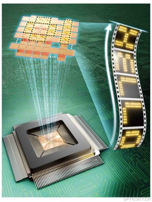
Figure 1. Schematic diagram of the design of a programmable optical nanoscale origami matrix.
To address this technological gap, the team at Beijing Institute of Technology has innovatively developed an addressable, programmable, megapixel‑scale electromechanically reconfigurable optical nano‑origami matrix (Fig. 1). This design is based on a deformable polyline‑based unit cell, which significantly enhances the optical contrast for information encryption and display. It enables the concealment and reconstruction of multiple custom patterns through two distinct structural encodings. With a unit cell period of only 2.5 μm, this work provides an important technical reference for the miniaturization of spatial light modulation devices and systems, such as microdisplays, optoelectronic chips, intelligent machine vision systems, and hyperspectral image sensors.
In practical applications of information encoding and display, achieving independent, real-time programmable control of individual pixels is of great significance. To demonstrate this capability, the research team has proposed a high‑contrast, pixelated, electromechanically reconfigurable design based on the Multi‑Line Addressing (MLA) strategy. By integrating a nano‑origami matrix with programmable electrodes into an optoelectronic modulation chip, they have successfully realized a freely programmable optical display comprising 10,000 pixels, thereby opening up a new technological pathway for the development of high‑performance, multifunctional microdisplay devices.
To further demonstrate the feasibility of fabricating and programmably controlling ultra‑large‑pixel‑scale nano‑origami arrays, the research team designed a spiral‑shaped nano‑origami structure to create a low‑voltage‑driven, strip‑type optoelectronic modulation chip. Limited by experimental constraints, this chip incorporates only 200 independent top‑layer electrodes; however, each electrode hosts 19,350 spiral‑shaped nano‑origami units, yielding a record‑breaking total of 3,870,000 deformable pixels—exceeding the 3,686,400 pixels of a 1440p QHD display (four times the resolution of Full HD). To validate its programmable modulation capabilities, the experiments further showcased its optical information‑transmission properties, including encrypted displays in Morse code and an optical “piano performance” demonstration. In addition, the team employed a custom‑built optical projector to demonstrate the device’s ability to project tailored patterns and megapixel‑scale nano‑origami arrays, highlighting the potential of optical nano‑origami arrays for miniaturized optical devices. Looking ahead, by integrating spatiotemporal encoding and high‑speed control technologies, this approach could open up new application avenues for multifunctional spatial light‑modulation chips.
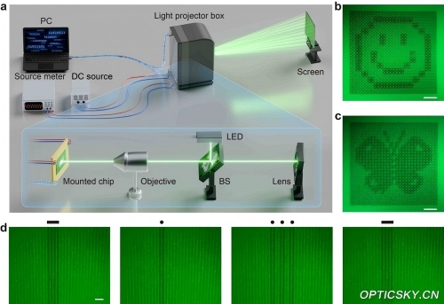
Figure 2. Demonstration of freely controllable optical projection based on a nano‑paper‑cutting matrix.
In summary, this work innovatively designs a high‑duty‑cycle nano‑origami architecture and successfully fabricates a megapixel‑scale integrated optical nano‑origami matrix, enabling electromechanically programmable optical information encryption and display with an ultra‑large pixel count and sub‑micron pixel dimensions. This advances the state of the art in areas such as micro‑display technology, optoelectronic chips, intelligent machine vision, and hyperspectral imaging, offering novel research directions and technical pathways for further innovation.
Source: Beijing Institute of Technology
LATEST NEWS
Thank you for visiting the official website of Chongfan Technology. If you have cooperation intentions or suggestions, please contact us through the following methods, and we will reply as soon as possible, thank you!
Address: Room 403, Building 6, Phase III of R&D, No. 36 Xiyong Avenue, High tech Zone, Chongqing, China.
Telephone: +86-13658337211
E-mail: Sales@cfkeji.net
Website: www.cfkeji.net
Mobile Version