Chongfan Technology
Products
Product

Chessboard grating
Classification:
Detail
Parameters
Technical Data
● With linearly polarized light incidence, a 2×2 uniform beam splitter can be achieved.
● Checkerboard phase structure, with a phase difference of π between adjacent pixel cells.
● Flat-panel structure, high uniformity, and low zero‑level defect rate
● Liquid crystal polymer/N-BK7 window material, without a mechanical housing, with a 1.5 mm bevel on one side
● Operating wavelengths: 532, 633, and 1064 nm; pixel size: 36 × 36 μm
● Supports flexible customization of parameter specifications
Chongfan Technology’s Checkerboard Grating (CG) is fabricated on an N‑BK7 glass substrate and incorporates liquid crystal polymers (LCP), a birefringent material. It features a sandwich‑type structure consisting of front and rear glass substrates with an LCP functional layer in between, without a mechanical housing, and includes a 1.5 mm edge cut on one side. Within the LCP layer, liquid crystal molecules are aligned in a checkerboard‑like pattern: the orientation angle is uniform across each pixel cell, while the phase difference between adjacent cells is π. This results in a consistent λ/2 retardance across the entire device plane, making it a single‑wavelength component. The checkerboard grating is primarily used to achieve uniform 2×2 beam splitting; compared with the three‑element cascaded grating design, it can accomplish 2×2 splitting with a single element, offering greater ease of integration. LBTEK offers standard checkerboard gratings operating at wavelengths of 532 nm, 633 nm, and 1064 nm, with a pixel size of 36 × 36 μm, and also provides flexible customization of parameters to meet diverse application requirements. For more details, please contact Chongfan Technology’s technical support.


Chessboard grating
● Optical component materials: liquid crystal polymer / N-BK7 window substrate
● Clear Aperture: 15 mm × 15 mm
● Operating wavelengths: 532 nm, 633 nm, 1064 nm
Chongfan Technology’s grating plates are fabricated on N‑BK7 window substrates, featuring a double‑layer design with a total thickness of 3.2 mm. They maintain a uniform phase retardation across the entire clear aperture, equal to half the operating wavelength. At the design wavelength, the outgoing light from adjacent pixels exhibits a phase difference of π, thereby generating a well‑defined diffraction pattern. Chongfan Technology offers a range of customization services; please contact our technical support team for further details.

Microscopic structure diagram of the chessboard grating

Chongfan Technology Chessboard Grating – Technical Description
I. Overview
Chongfan Technology’s checkerboard grating (CG) is a two-dimensional 0–π phase‑shift grating composed of alternating deflections of liquid‑crystal pixels of identical size. It primarily employs optical phase‑shifting techniques to fabricate, on a glass substrate, liquid‑crystal polymer films with alternately arranged 0–π phase shifts. By precisely controlling the thickness of these liquid‑crystal polymer films, the optical path difference between the ordinary (o) and extraordinary (e) rays is tuned to be an odd multiple of half the wavelength (i.e., a λ/2 retardance), thereby enabling its beam‑splitting functionality.
Checkerboard gratings are primarily used to achieve uniform 2×2 beam splitting, and compared with the three‑element cascaded grating design, a single checkerboard grating can accomplish 2×2 splitting, making it easier to integrate. Owing to their advantages—such as two‑dimensional beam splitting, low zero‑order efficiency, and high uniformity—checkerboard gratings are widely employed in applications like microsurface topography measurement and wavefront sensing.
II. Product Appearance and Structure
Chongfan Technology’s grating plates are fabricated using liquid crystal polymer birefringent material and an N‑BK7 glass substrate, featuring a typical sandwich structure of “front and rear glass substrates with an intermediate LCP functional layer.” They come without a mechanical housing and have a beveled edge on one side to indicate the beam‑splitting direction.
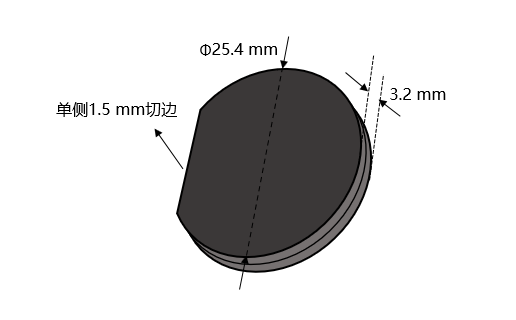
Figure 1: External Appearance and Structural Diagram of the Checkerboard Grating Product
- The Daman grating element measures Ø25.4 × 3.2 mm, is a bare chip, and comes without a mechanical housing.
- One side features a trimmed edge with a width of 1.5 mm; the trimming direction is parallel to one side of the square light‑transmitting aperture, serving to indicate the beam‑splitting orientation.
III. Optical Properties
1. The checkerboard grating features a checkerboard‑type phase structure, with a phase difference of π between adjacent pixel cells, enabling phase modulation of the laser beam and achieving 2×2 beam splitting.
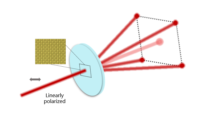
Figure 2: Schematic of the grating phase structure and beam splitting on the chessboard.
- Note: The structural diagram at the center of the component shown in the figure is an actual photograph taken under a polarizing microscope. In reality, the fast‑axis orientation of the liquid‑crystal molecules ranges from 0° to 90°, resulting in a distinct bright–dark contrast. However, when observed with a polarizing microscope, because the coating on the component introduces a retardance of λ/2, the polarization direction of the linearly polarized light exiting the component is rotated by twice the angle relative to the fast axis. Consequently, what we actually observe spans 0° to 180°, yielding a much more uniform brightness distribution.
2. Due to the grating’s unique binary‑symmetric structure, it is highly sensitive to even minute structural errors. When the random deviations in the structure reach the order of 5 μm, distinct connecting lines can be observed between adjacent diffraction spots in the diffraction pattern.
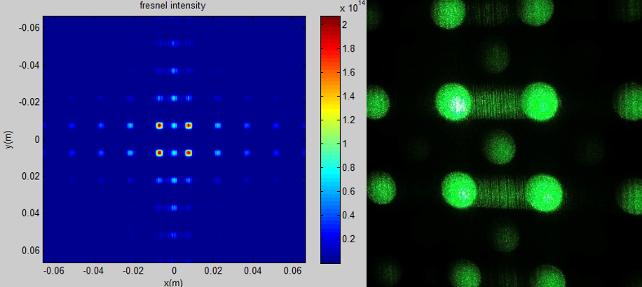
Figure 3 Schematic diagram of grating‑based wiring simulation and experimental measurement on the chessboard
3. The grating on the Chongfan Technology chessboard can achieve a diffraction efficiency close to that predicted by theoretical simulations (with a theoretical first-order diffraction efficiency of 65.6% and an actual first-order diffraction efficiency exceeding 60%), and exhibits no spurious coupling between its first-order diffraction orders.
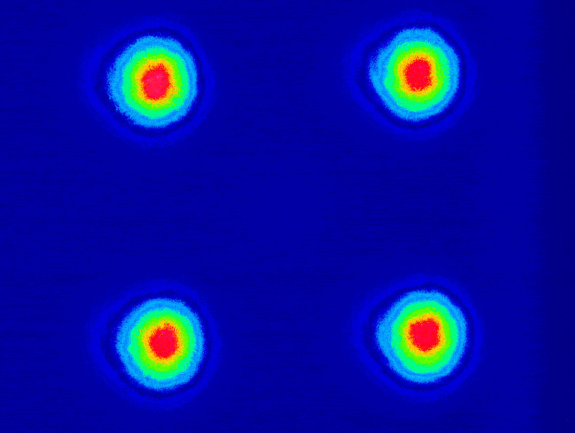
Figure 4: Measured performance of the grating beam quality analyzer (diffraction efficiency: 61.8%, uniformity: 98.25%)
IV. Parameter Description
1. Diffraction efficiency and beam-splitting uniformity
The figure below shows the optical setup for measuring the energy of the diffracted spot when linearly polarized light is normally incident on a checkerboard grating. The diffracted‑spot energy is predominantly concentrated in the ±1st diffraction orders, with a relatively uniform intensity distribution (non‑uniformity < 5%), while the energy of the zeroth‑order spot accounts for less than one thousandth of the total. Based on this measurement configuration, the diffraction efficiency and beam‑splitting uniformity of the checkerboard grating are defined as follows:
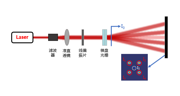
Figure 5: Optical path diagram for grating testing on the chessboard
- Diffraction efficiency: defined as the ratio of the total energy of the ±1st-order diffracted beams to the total incident light intensity transmitted through the grating.
- Beam‑splitting uniformity: Uniformity is defined as the ratio of the difference between the maximum and minimum energy spots in a ±1st‑order diffracted spot to the sum of the energies of these two spots; thus, uniformity = 1 − non‑uniformity.
- Zero-order energy fraction: defined as the ratio of the energy of the zero-order diffracted spot to the total light intensity transmitted through the grating.
2. Damage Threshold
Based on the strong absorption characteristics of LCP materials in the short‑wave region, the damage threshold of a checkerboard grating increases as its operating wavelength becomes longer. According to experimental measurements, the reference value for the damage threshold of Chongfan Technology’s checkerboard gratings is:
- 33.6 mJ/cm² @ 532 nm, 8.69 ns, 9.84 Hz; (fused silica substrate)
- 1.379 mJ/cm² @ 1064 nm, 14.605 ps, 300 kHz; (fused silica substrate)
- 0.0735 mJ/cm² @ 1064 nm, 500 fs, 300 kHz; (fused silica substrate)
- 1.4 kW/cm² at 1064 nm, CW. (Fused silica substrate)
Previous
Previous
Other Products
I want to consult
Thank you for visiting the official website of Chongfan Technology. If you have cooperation intentions or suggestions, please contact us through the following methods, and we will reply as soon as possible, thank you!
Address: Room 403, Building 6, Phase III of R&D, No. 36 Xiyong Avenue, High tech Zone, Chongqing, China.
Telephone: +86-13658337211
E-mail: Sales@cfkeji.net
Website: www.cfkeji.net
Mobile Version