Chongfan Technology
News
01
2026
-
06
Molnar Nanophotonics: From Fundamental Concepts to Device Engineering
Author:
The team of Haoning Tang at MIT, in collaboration with the group of Igor Aharonovich at the University of Technology Sydney, has systematically reviewed in a recent survey the fundamental physical mechanisms of moiré nanophotonics, the progress of representative devices, and future directions for engineering applications. Moiré photonic structures generate long-range superstructures through relative rotation, translation, or parameter mismatch among periodic units, thereby offering new geometric degrees of freedom for tuning optical band structures, local density of states, radiative losses, and momentum‑transfer pathways.
This review focuses on band folding, interlayer hybridization, flat-band formation, and light-field localization mechanisms in twisted bilayer photonic crystals and moiré superlattices. Unlike conventional photonic crystals with fixed geometries, moiré platforms enable continuous tuning of optical responses—without redesigning the overall structure—by adjusting the twist angle, stacking configuration, and interlayer coupling. This unique feature allows for the realization of high‑Q, small‑mode‑volume moiré photonic cavities and provides a novel device platform for applications such as low‑threshold nanolasers, collective coherent lasers, cavity quantum electrodynamics, nonlinear frequency conversion, beam shaping, and vortex‑light generation.
The article further notes that moiré nanophotonics is transitioning from fundamental proof-of-concept studies to device engineering. In the future, by integrating high-precision nanofabrication, two-dimensional materials, quantum emitters, nonlinear optical materials, and MEMS‑based reconfigurable platforms, moiré photonic structures hold promise for evolving into a new generation of nanophotonic devices that are manufacturable, integrable, and dynamically tunable.
This achievement was published in Optica on May 22, 2026, under the title “Moiré nanophotonics: from fundamental concepts to device engineering.”
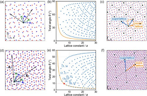
Figure 1: Construction of commensurate moiré superlattices in twisted square and hexagonal lattices.
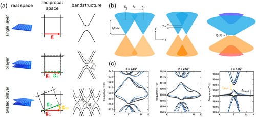
Figure 2: Band folding and interlayer hybridization mechanisms in twisted bilayer photonic crystals.
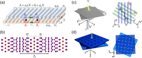
Figure 3: Two types of dispersion-engineering strategies in one-dimensional and two-dimensional moiré photonic structures: parameter‑mismatched superlattices and twist‑induced superlattices.
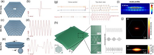
Figure 4: Comparison of the localized modes among the Moiré photonic cavity, the conventional defect cavity, and the BIC photonic crystal slab.
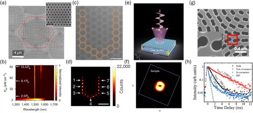
Figure 5: Representative advances in moiré photonic crystal lasers, collective lasers, and cavity quantum electrodynamics.
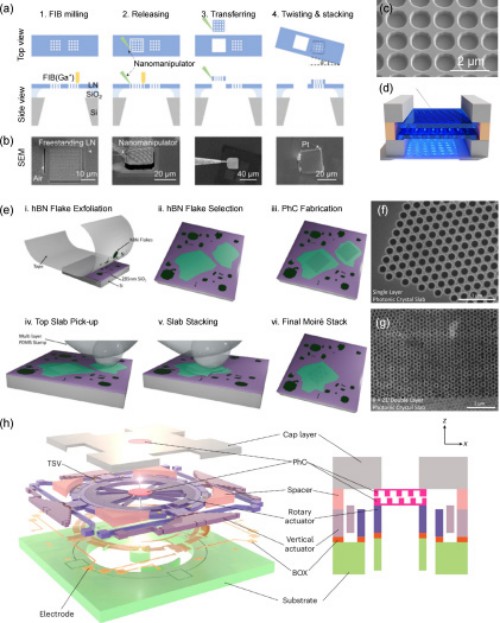
Figure 6: Typical fabrication, transfer, stacking, and MEMS‑based reconfigurable implementation schemes for a twisted bilayer photonic lattice.
Source: Optics World
Previous
Previous
LATEST NEWS
Thank you for visiting the official website of Chongfan Technology. If you have cooperation intentions or suggestions, please contact us through the following methods, and we will reply as soon as possible, thank you!
Address: Room 403, Building 6, Phase III of R&D, No. 36 Xiyong Avenue, High tech Zone, Chongqing, China.
Telephone: +86-13658337211
E-mail: Sales@cfkeji.net
Website: www.cfkeji.net
Mobile Version