Chongfan Technology
News
19
2025
-
05
Obsidian's revolutionary glass-based MEMS manufacturing platform achieves SVGA infrared thermal imaging sensors
Author:
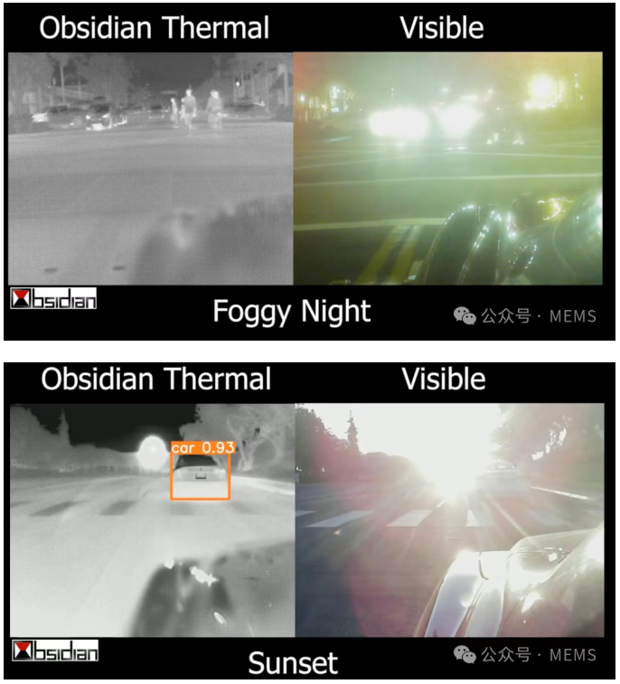
According to MEMS Consulting, Obsidian Sensors recently announced the launch of a new “glass-based” high-resolution infrared thermal imaging sensor with SVGA (800 x 600 pixels) resolution and a pixel pitch of 17 micrometers. This new sensor is manufactured by Obsidian Sensors’ manufacturing partner, Innolux, on large glass substrates at its T3 LTPS fab in Zhunan, Taiwan. In a very short time, Obsidian Sensors expanded the pixels to the 17-micron node, increasing the sensor’s resolution by more than 50%, which fully demonstrates the close and efficient cooperation between Obsidian Sensors and Innolux.
Obsidian Sensors stated: “While our competitors are struggling to meet the mass market (adopting aggressive price targets) by reducing the resolution of infrared thermal imaging sensors, Obsidian Sensors is fully leveraging our revolutionary manufacturing platform to produce higher-resolution infrared thermal imaging sensors at the same price. This SVGA sensor uses wafer-level vacuum packaging and has a size very similar to our existing VGA sensors that have shipped to numerous customers worldwide.”
With JDI (Japan Display Inc.) becoming our second manufacturing partner, Obsidian Sensors will consolidate its position to enhance the competitiveness of infrared thermal imaging products with unprecedented pixel scale and price, which is exactly what the world needs in many aspects today. John Hong, CEO and co-founder of Obsidian Sensors, said: “SVGA microbolometer focal plane arrays will be available to customers later this year. We plan to launch SXGA (1280 x 1024 pixels) resolution, 12-micron infrared thermal imaging sensors in 2026 to meet the most demanding applications, including thermal imaging applications for military and civilian robots.”
For most people working with infrared thermal imaging, the choice between “silicon substrate” and “glass substrate” is still unclear. But today, we have eliminated all technical risks of manufacturing on large glass substrates and have successfully achieved high-yield glass-based microbolometer focal plane arrays. John Hong said: “We are focused on executing our development roadmap, striving to achieve SXGA (1280 x 1024 pixels) resolution in 2026, FHD (1920 x 1080 pixels) resolution in 2027, and 4K (3840 x 2160 pixels) resolution in 2028. As a true dual-use technology, we serve not only the commercial markets in automotive, security, and industrial sectors but also the defense market that uses commercial components.”
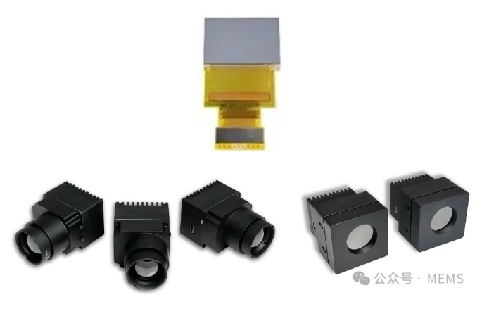
Headquartered in San Diego, California, Obsidian Sensors was spun out of Qualcomm in 2017 to develop and produce a new type of microbolometer focal plane array based on glass substrates, using flat panel display manufacturing equipment. Obsidian Sensors’ LAMP (Large Area MEMS Platform) manufacturing technology is a surface micromachining process that integrates high-performance LTPS TFT (Low-Temperature Polysilicon Thin-Film Transistor) for manufacturing microbolometers and other MEMS devices at the lowest cost and highest yield.
LATEST NEWS
2025-06-06
Photonic avalanche nanocrystals with >500-order optical nonlinear response
At the forefront of nonlinear optical materials research, photon avalanche (PA), a unique luminescence mechanism occurring in lanthanide-ion-doped systems, exhibits exponential response under continuous laser pumping through an energy positive feedback loop mechanism, thus demonstrating ultra-high-order nonlinear optical behavior far exceeding traditional upconversion processes.
2025-06-05
Ji Xingchen/Su Yikai LPR | 780 nm on-chip integrated high-Q ultra-wideband Fabry-Perot cavity
With the rapid development of applications such as quantum precision measurement, atom manipulation, and narrow linewidth lasers, higher and higher demands are placed on high-performance photonic devices operating in the visible and near-visible wavelength range (especially the 780 nm wavelength corresponding to the rubidium atomic transition).
2025-06-23
Binary optics and metasurface lenses
Bichromatic optics is a subject or an optical technology; the concept of a meta-lens is more inclined to be a device.
2025-06-23
Achromatic diffractive waveguide in AR glasses
AR glasses seem to have developed rapidly in recent years; many believe this is the device most likely to replace mobile phones in the future.
Thank you for visiting the official website of Chongfan Technology. If you have cooperation intentions or suggestions, please contact us through the following methods, and we will reply as soon as possible, thank you!
Address: Room 403, Building 6, Phase III of R&D, No. 36 Xiyong Avenue, High tech Zone, Chongqing, China.
Telephone: +86-13658337211
E-mail: Sales@cfkeji.net
Website: www.cfkeji.net
Mobile Version