Chongfan Technology
News
05
2025
-
06
Ji Xingchen/Su Yikai LPR | 780 nm on-chip integrated high-Q ultra-wideband Fabry-Perot cavity
Author:
With the rapid development of applications such as quantum precision measurement, atom manipulation, and narrow-linewidth lasers, increasingly high demands are placed on high-performance photonic devices operating in the visible and near-visible wavelength bands (especially the 780 nm wavelength corresponding to the rubidium atomic transition). Among them, Fabry-Pérot (F-P) resonators with high quality factor (Q factor) and large bandwidth are important devices for realizing atomic photonics and narrowband lasers. However, in the visible and near-visible wavelength bands, traditional on-chip integrated F-P cavities face limitations such as high material absorption, complex reflector structures, and waveguide processing precision, making it difficult to balance high Q factor, large bandwidth, and manufacturing robustness.
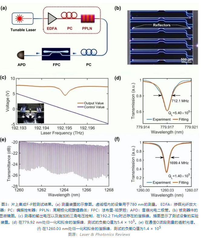
To solve this problem, Associate Professor Ji Xingchen and Professor Su Yikai from the Optical Transmission and Integrated Photonics Laboratory (OTIP) of the School of Electronic Information and Electrical Engineering, Shanghai Jiao Tong University proposed and verified an integrated F-P cavity suitable for the 780 nm band with ultra-large bandwidth and high manufacturing tolerance. This device uses a silicon nitride (SiN) platform, combined with a novel triangular reflection structure and mode conversion coupler, to achieve an intrinsic Q value of 6.1 × 10 5 without thermal annealing, with a working bandwidth exceeding 500 nm, setting a new record for on-chip integrated F-P cavities in this band. It provides important technical support for on-chip atom cooling, quantum optics, and other applications.
Design Ideas and Working Principles
F-P cavities form standing wave resonance through mirrors at both ends, effectively enhancing the interaction between light and matter. In the communication C-band, on-chip integrated F-P cavities based on silicon-on-insulator (SOI) have made significant progress. However, in the visible and near-visible wavelength bands (such as 780 nm), traditional silicon-based platforms are limited by the high loss of silicon waveguides, short Bragg structure periods, and small process tolerances, making it difficult to achieve high-Q on-chip integrated F-P cavities. In this paper, a silicon nitride on insulator (SiNOI) platform is used, relying on its wide transparent window, low loss, and good process compatibility, providing a solid foundation for the realization of high-performance F-P cavities.
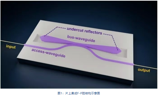
To overcome the above limitations, this study designed an integrated F-P cavity structure based on an isosceles right-angled triangular reflector (IRTR) and an asymmetric directional coupler (ADC). This cavity combines the propagation of TE 1 modes and the total internal reflection structure, ensuring high reflectivity (>0.98) while effectively improving the cavity's tolerance to processing deviations (such as sidewall tilt and waveguide width variations). Test results show that the intrinsic Q value of this structure at a wavelength of 780 nm is 6.1 × 10 5 , which is the highest record known for on-chip integrated F-P cavities in this band. In addition, the device maintains a Q value higher than 10 at 1260 nm 5 , demonstrating a wideband operating capability exceeding 500 nm.
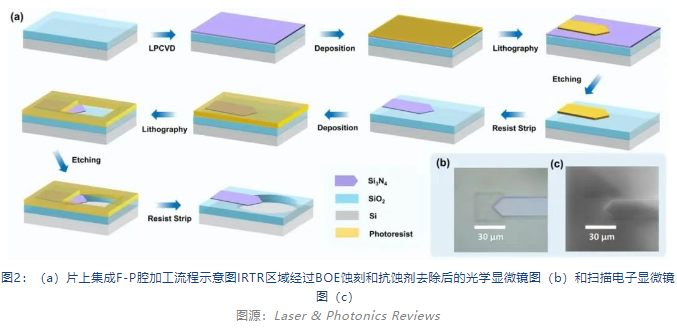
The device structure consists of three parts: an asymmetric directional coupler for mode conversion and selective coupling, an adiabatic tapered waveguide to ensure TE 1 mode propagation with low loss between the reflectors, and an IRTR reflector to achieve total internal reflection through the air cladding and provide high reflectivity. The team used LPCVD deposition technology combined with electron beam lithography and plasma etching technology to complete the device fabrication, and achieved high-sensitivity Q-value measurement through equipment such as frequency-doubled lasers and photodetectors. This design avoids complex Bragg grating structures, simplifies the process flow, significantly improves the working bandwidth, and provides a new solution for future on-chip integrated broadband high-Q optical resonators.
Summary and Outlook
This study successfully achieved for the first time an on-chip integrated F-P cavity with high Q factor, ultra-large bandwidth, and high manufacturing tolerance in the 780 nm band, effectively breaking through the bottleneck in design and manufacturing in the visible/near-visible wavelength band. The high versatility and good process compatibility of this structure provide great potential for applications such as on-chip rubidium atom cooling, narrow-linewidth lasers, and quantum information processing.
Looking to the future, the research team will actively promote the practical application of this device, including integration with on-chip lasers, modulators, and detectors, and will continue to explore other innovative solutions for achieving high-Q on-chip integrated F-P cavities in the visible/near-visible wavelength band. This will help to promote the industrialization and application of the next generation of photonic chips and quantum devices, opening up new frontiers for the development of photonics and quantum technology.
LATEST NEWS
2025-07-12
Hyperspectral channel density on-chip diffractive speckle spectrometer
Driven by the demand for high-performance miniature spectrometers, research on chip-scale spectrometers is continuously breaking through towards high integration, high resolution, and large bandwidth. This work proposes a silicon-based on-chip spectrometer based on cascaded disordered metasurfaces. Through various on-chip wavefront modulation mechanisms, high-spectral speckle is generated, which expands the number of spectral channels with a compact chip size, thus achieving extremely high on-chip spectral channel density and providing an effective means for achieving high-resolution, large-bandwidth spectral detection.
2025-07-14
Ultrasensitive room-temperature extreme photoelectric response achieved
This study, for the first time, achieved the control of ultra-sensitive photoelectric response optimized for room temperature conditions through electromagnetically induced potential well effects and exciton insulator phase transition characteristics.
2025-07-15
Preparation and research progress of glass scintillators for X-ray imaging
Developing suitable host materials with strong X-ray absorption coefficient, good exciton transport efficiency, low phonon energy, and high lanthanide ion solubility remains a cutting-edge research direction in the field of X-ray detection.
2025-07-16
Quantum logic gates based on single-piece gradient metasurface
In today's rapidly developing quantum information technology, realizing efficient and highly integrated quantum logic gates is one of the key challenges in the field of integrated quantum optics.
2025-07-17
Preparation and performance study of epoxy-thiol high-contrast color polymer dispersed liquid crystals
Polymer Dispersed Liquid Crystal (PDLC) is a smart material consisting of micron-sized liquid crystal droplets dispersed in a polymer matrix.
Thank you for visiting the official website of Chongfan Technology. If you have cooperation intentions or suggestions, please contact us through the following methods, and we will reply as soon as possible, thank you!
Address: Room 403, Building 6, Phase III of R&D, No. 36 Xiyong Avenue, High tech Zone, Chongqing, China.
Telephone: +86-13658337211
E-mail: Sales@cfkeji.net
Website: www.cfkeji.net
Mobile Version