Chongfan Technology
News
21
2025
-
05
Quantum Dot Short-wave Infrared Image Sensor based on p-n homojunction
Author:
Quantum dot (QD)-based photodetectors are promising alternatives for low-cost construction of short-wave infrared (SWIR) image sensors. Improving the photoresponse and scalability of quantum dots is crucial for their practical applications. Existing quantum dot photodetectors face pixel uniformity issues caused by vertical p-n junctions, which lead to significant pixel-to-pixel variations, and the vertical structure limits the ability to achieve higher resolution and smaller pixel sizes.
According to MEMS Consulting, recently, research teams from Westlake University and Zhejiang University have developed a complementary metal-oxide-semiconductor (CMOS)-compatible short-wave infrared image sensor based on lead sulfide (PbS) quantum dots, utilizing a p-n homojunction photoconductor architecture. A p-n homojunction was constructed by combining solution-phase ligand-exchanged PbS quantum dots treated with lead iodide (PbI₂) and solid-state ligand-exchanged PbS quantum dot films treated with ethanedithiol (EDT), which more effectively separates photogenerated carriers and significantly enhances photoresponse. This method enables monolithic integration of solution-processed quantum dots with silicon readout integrated circuits (ROIC) without complex flip-chip bonding, and facilitates large-scale manufacturing (640 × 512) of quantum dot image sensors. Consequently, the homojunction-based quantum dot short-wave infrared image sensor exhibits low-noise performance and high average detectivity, and its ability to capture high-resolution short-wave infrared images highlights its potential in various applications. This research was published in ACS Photonics under the title "Quantum Dots Short-Wave Infrared Image Sensor with Enhanced Photoresponse Enabled by a Planar p–n Homojunction".
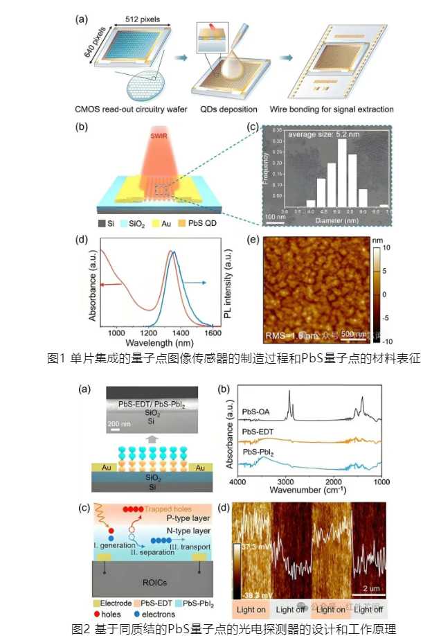
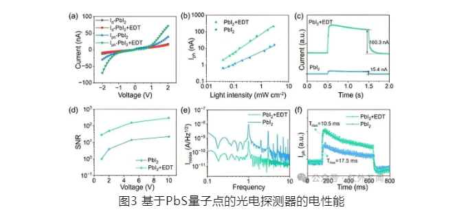
Figure 1a shows a schematic diagram of the monolithic integration of a quantum dot photodetector with a CMOS readout integrated circuit. Figure 1b shows a schematic diagram of a homojunction-based PbS quantum dot photodetector. Researchers characterized the device using high-resolution transmission electron microscopy (HRTEM), absorption spectroscopy, photoluminescence (PL) spectroscopy, and atomic force microscopy (AFM). Figure 2a shows the configuration of the bilayer photodetector, and Figure 2c illustrates the working mechanism of the p-n homojunction-based PbS quantum dot photodetector.
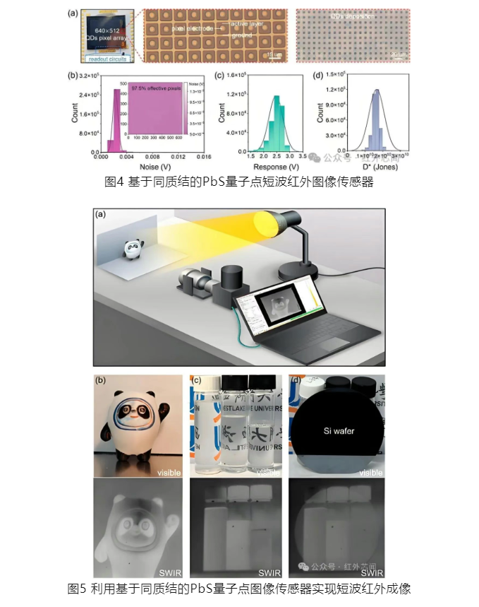
Subsequently, the researchers fabricated photodetectors based on single-layer (PbS-PbI₂) and bilayer (PbS-PbI₂ + EDT) quantum dot films and tested their optoelectronic properties, thereby demonstrating the advantages of the p-n homojunction. The relevant results are shown in Figure 3.
Then, the researchers successfully monolithically integrated PbS quantum dots with a readout integrated circuit consisting of 640 × 512 pixels to form a short-wave infrared image sensor, as shown in Figure 4. The researchers used this short-wave infrared image sensor to achieve short-wave infrared imaging, and the imaging results are shown in Figure 5.
In summary, this study developed a p-n homojunction-based PbS quantum dot photodetector. The n-type PbS-PbI ₂ film and p-type PbS-EDT film combination enables self-driven photocarrier separation and accumulation, significantly reducing carrier recombination and enhancing photocurrent. Compared to vertical photodiode configurations, this design is fully compatible with silicon readout integrated circuits, effectively reducing manufacturing complexity and minimizing deposition non-uniformity. Therefore, obtaining high-resolution short-wave infrared image sensors shows great potential in various applications such as chemical analysis and semiconductor inspection. The p-n homojunction-based photodetector proposed in this study provides a convenient method for developing planar quantum dot image sensors, marking a significant advancement for next-generation short-wave infrared image sensors.
LATEST NEWS
2025-06-06
Photonic avalanche nanocrystals with >500-order optical nonlinear response
At the forefront of nonlinear optical materials research, photon avalanche (PA), a unique luminescence mechanism occurring in lanthanide-ion-doped systems, exhibits exponential response under continuous laser pumping through an energy positive feedback loop mechanism, thus demonstrating ultra-high-order nonlinear optical behavior far exceeding traditional upconversion processes.
2025-06-05
Ji Xingchen/Su Yikai LPR | 780 nm on-chip integrated high-Q ultra-wideband Fabry-Perot cavity
With the rapid development of applications such as quantum precision measurement, atom manipulation, and narrow linewidth lasers, higher and higher demands are placed on high-performance photonic devices operating in the visible and near-visible wavelength range (especially the 780 nm wavelength corresponding to the rubidium atomic transition).
2025-06-23
Binary optics and metasurface lenses
Bichromatic optics is a subject or an optical technology; the concept of a meta-lens is more inclined to be a device.
2025-06-23
Achromatic diffractive waveguide in AR glasses
AR glasses seem to have developed rapidly in recent years; many believe this is the device most likely to replace mobile phones in the future.
Thank you for visiting the official website of Chongfan Technology. If you have cooperation intentions or suggestions, please contact us through the following methods, and we will reply as soon as possible, thank you!
Address: Room 403, Building 6, Phase III of R&D, No. 36 Xiyong Avenue, High tech Zone, Chongqing, China.
Telephone: +86-13658337211
E-mail: Sales@cfkeji.net
Website: www.cfkeji.net
Mobile Version