
Chongfan Technology
News
18
2025
-
05
Xiangtan University develops self-powered, broadband, and polarization-sensitive photodetectors, aiding near-infrared polarization detection.
Author:
A Schottky junction, as a metal-semiconductor contact structure, is widely used in electronic and optoelectronic devices due to its excellent rectification and photovoltaic properties. Schottky junction photodetectors utilize built-in electric fields to efficiently separate photogenerated carriers, showing great potential in self-powered, ultra-sensitive, and fast-response photodetectors. However, problems such as Fermi level pinning effect, interface defect states, and reverse leakage current of back-to-back Schottky junctions in the preparation process of traditional metal electrodes pose challenges to the precise regulation of Schottky barrier and the optimization of rectification performance. The development of two-dimensional (2D) materials brings new opportunities for photodetectors, especially 2D semimetals, whose interlayer Van der Waals interactions can significantly alleviate the Fermi level pinning effect and strictly follow the Schottky-Mott rule, thereby enabling precise regulation of the Schottky barrier height. In addition, 2D semimetals also possess zero-bandgap characteristics, anisotropy, and unique topologically protected band structures, giving them significant competitive advantages in self-powered, polarization-sensitive, and broadband photodetection applications.
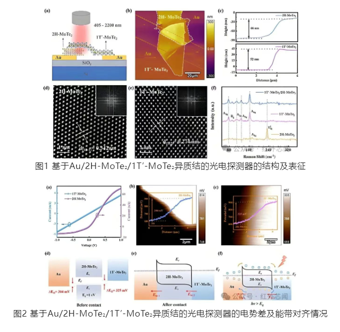
This study constructed a vertical heterojunction structure of Au/2H-MoTe₂/1T’-MoTe₂ and developed self-powered, broadband, and polarization-sensitive photodetectors using asymmetric Schottky contacts. This vertical structure shortens the diffusion distance of carriers within the heterojunction, improving carrier separation efficiency. First, Au electrodes were deposited on SiO₂/Si substrates by ion sputtering. Then, 2H-MoTe₂ and 1T’-MoTe₂ nanosheets were exfoliated from bulk crystals using blue tape and transferred to the substrate with the aid of polydimethylsiloxane (PDMS). The thickness and surface potential images of the heterojunction were measured using atomic force microscopy (AFM), high-resolution images of 1T’-MoTe₂ and 2H-MoTe₂ nanosheets were obtained by transmission electron microscopy (TEM), and the Raman spectrum of the heterojunction was collected using a Raman spectrometer. Relevant results are shown in Figure 1 and Figure 2. Through experiments and characterization, the significant role of 1T’-MoTe₂ in alleviating the Fermi level pinning effect was verified.
Next, the researchers conducted a comprehensive analysis of the optoelectronic performance of the photodetector based on the Au/2H-MoTe₂/1T’-MoTe₂ heterojunction. Figure 3 shows the optoelectronic performance of the device in dark state and under 1064 nm illumination (near-infrared). Figure 4 shows the optoelectronic performance of the device under 660 nm illumination (visible light). The results show that by constructing two built-in electric fields in the same direction, the driving force for photogenerated carrier separation was significantly enhanced, thereby improving the photodetector performance of the heterojunction, achieving broadband photodetection from 405 nm to 2200 nm; under 660 nm laser illumination, its peak On/Off ratio was 5.97×10⁴, responsivity was 80.59 mA/W, external quantum efficiency was 15.14%, and specific detectivity was 1.05×10¹² Jones.

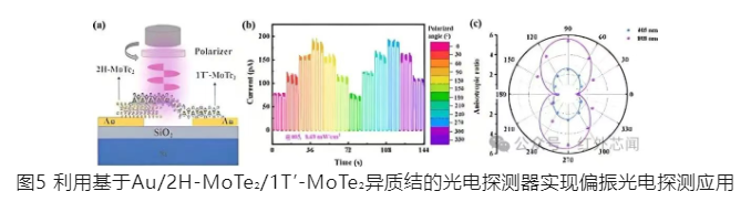
In summary, this study successfully developed a Au/2H-MoTe₂/1T’-MoTe₂ heterojunction based on asymmetric Schottky contacts, achieving self-powered, broadband, and polarization-sensitive photodetection. By introducing 1T’-MoTe₂, the Fermi level pinning effect was significantly alleviated, rectification performance was improved, and carrier separation efficiency was enhanced by two built-in electric fields in the same direction. This heterojunction exhibited excellent photodetection performance in the 405 nm to 2200 nm wavelength range, especially under 660 nm laser illumination, where its key parameters such as On/Off ratio, responsivity, external quantum efficiency, and specific detectivity all performed exceptionally well. This research not only provides new ideas for the development of self-powered, broadband, and polarization-sensitive photodetectors but also offers important insights for the application of 2D Van der Waals semimetals in high-performance optoelectronic devices.
LATEST NEWS
Thank you for visiting the official website of Chongfan Technology. If you have cooperation intentions or suggestions, please contact us through the following methods, and we will reply as soon as possible, thank you!
Address: Room 403, Building 6, Phase III of R&D, No. 36 Xiyong Avenue, High tech Zone, Chongqing, China.
Telephone: +86-13658337211
E-mail: Sales@cfkeji.net
Website: www.cfkeji.net
Mobile Version