Chongfan Technology
News
21
2026
-
05
Progress has been made in research on laser‑ceramic ion slicing and on‑chip amplifiers.
Author:
Recently, a team from the Shanghai Institute of Optics and Fine Mechanics of the Chinese Academy of Sciences has made progress in research on ion‑implanted Nd:YAG laser ceramics and their on‑chip amplifiers.
Submicron‑scale solid‑state laser gain films are essential for achieving high‑power on‑chip optical amplification. This study applies ion‑slicing technology to Nd:YAG laser ceramics and elucidates a dual mechanism by which grain boundaries contribute to stress relaxation during annealing. Experiments reveal that, in the low‑temperature range of 550–850 °C, helium ions accumulate along grain boundaries, forming bubbles that trigger grain‑boundary collapse; above 850 °C, helium atoms acquire sufficient kinetic energy to traverse grain boundaries, thereby initiating the cohesive delamination of the entire film layer. Based on these findings, a gradient annealing strategy is proposed—combining a 400 °C pre‑anneal with a rapid 900 °C post‑anneal—so that the pre‑anneal step prematurely releases the internal stresses required for grain‑boundary collapse, allowing the high‑temperature stage to dominate the overall delamination process. This approach enables the controlled transfer of ceramic thin films, with thicknesses of 915 nm and lateral dimensions on the order of hundreds of micrometers, onto sapphire substrates.
The transferred thin film was systematically characterized using transmission electron microscopy, atomic force microscopy, and photoluminescence spectroscopy. TEM images reveal a sharp, well-defined interface between the film and the substrate, with no dislocations or amorphous phases detected. AFM measurements indicate a surface roughness of approximately 2.5 nm. Photoluminescence spectra confirm that both the position and intensity of the dominant emission peak at 1064 nm are in excellent agreement with those of the bulk ceramic, demonstrating the nondestructive nature of the ion‑slice technique and its feasibility for device fabrication.
Based on an Nd:YAG ceramic–sapphire heterogeneous integration platform, the team designed and optimized a Si3N4 waveguide amplifier structure. Using finite-element simulations, they tuned the waveguide width, height, and gain-layer thickness to achieve mode confinement factors of 35.16% for the 808 nm pump light and 38.51% for the 1064 nm signal light. Simulation results indicate that, with a 12 cm waveguide length and a 160 mW pump power, the device can deliver a peak gain of approximately 25 dB at 1064 nm.
This work validates the feasibility of fabricating ceramic gain thin films using ion‑cutting technology and elucidates a dual‑path mechanism of stress relaxation mediated by grain boundaries, thereby offering a novel technological pathway for on‑chip integration of laser ceramic materials and the design of high‑performance waveguide amplifiers.
The relevant research findings were published in Materials & Design.
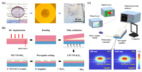
Process Flow and Subsequent Device Test Diagrams
Source: Shanghai Institute of Optics and Fine Mechanics
LATEST NEWS
Thank you for visiting the official website of Chongfan Technology. If you have cooperation intentions or suggestions, please contact us through the following methods, and we will reply as soon as possible, thank you!
Address: Room 403, Building 6, Phase III of R&D, No. 36 Xiyong Avenue, High tech Zone, Chongqing, China.
Telephone: +86-13658337211
E-mail: Sales@cfkeji.net
Website: www.cfkeji.net
Mobile Version