Chongfan Technology
News
02
2025
-
09
Artificial Intelligence Empowering Inverse Lithography Technology
Author:
Computational lithography technology improves resolution by optimizing process factors. Among them, Inverse lithography technology has attracted significant attention from academia and industry due to its global optimization characteristics. In recent years, artificial intelligence technology integration has brought new breakthroughs to inverse lithography, playing a role in lithography modeling, mask optimization, and other stages.
Recently, a research team from Tsinghua University published a paper titled " 'Advancements and challenges in inverse lithography technology: a review of artificial intelligence-based approaches' in 'Light: Science & Applications' reviewing AI-driven inverse lithography technology. The article summarizes the basic principles and development history of inverse lithography technology, analyzes the application of AI technology in inverse lithography, points out the challenges faced by inverse lithography technology, and looks forward to its development directions.
The corresponding author of this paper is Professor Liangcai Cao from Tsinghua University, and the first author is PhD student Yixin Yang from Tsinghua University. Associate Professor Chen Wang, PhD students Kexuan Liu and Yunhui Gao from Tsinghua University made important contributions to the paper.
Computational lithography
Lithography process main steps include coating, pre-baking, exposure, post-baking, development, etching, stripping, and inspection (Figure 1). Lithography exposure systems include contact, proximity, and projection types. Contact exposure has issues of mask contamination and damage, while proximity exposure accuracy is limited by wafer flatness. The projection lithography machine was introduced in 1973, achieving pattern transfer through spatial projection of the mask pattern.
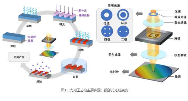
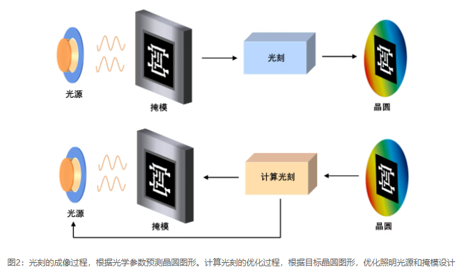
Lithography resolution enhancement technologies include off-axis illumination, optical proximity effect correction, phase-shift masks, etc. Computational lithography models the lithography imaging process and optimizes illumination sources and mask design based on the target wafer pattern (Figure 2).
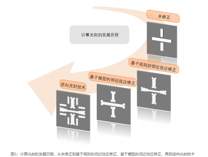
Computational lithography The main development stages include: rule-based proximity effect correction, model-based proximity effect correction, inverse lithography technology (Figure 3). Inverse lithography technology Based on lithography system models, using Hopkins theory and transmission cross coefficient to describe the optical imaging process, optimization problems are solved by gradient algorithms to make the predicted wafer pattern closely match the target pattern.
Research progress in inverse lithography technology
In 1981, researchers at the University of Wisconsin-Madison proposed a pixel-level mask optimization method. In 2003, Luminescent Technologies achieved industrial application of inverse lithography, and subsequently companies like Intel accelerated the commercialization of inverse lithography. In 2010, the introduction of regularization frameworks and conjugate gradient algorithms improved the computational efficiency of inverse lithography. In 2017, the integration of deep learning technology ushered in a new stage of inverse lithography development. Companies such as ASML adopted convolutional neural networks to accelerate optimization processes, and platforms like GPUs promoted the application of inverse lithography technology. Over more than forty years, inverse lithography has evolved from a theoretical concept to a key technology in semiconductor manufacturing (Figure 4).
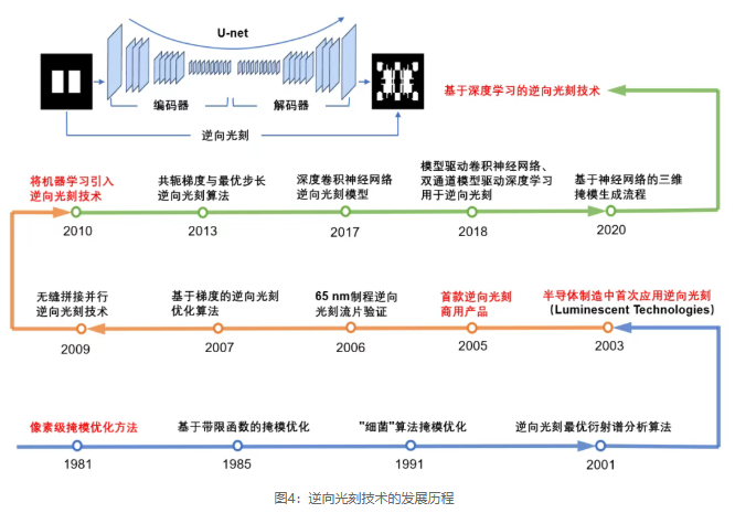
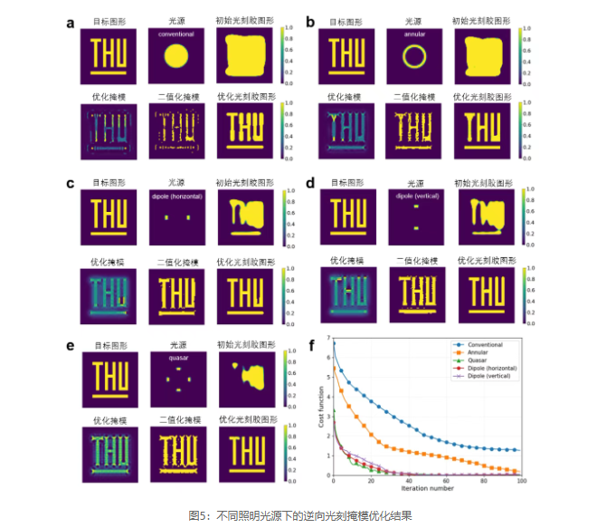
Figure 5 shows the mask optimization results of inverse lithography. Various illumination source modes can be used in computational lithography, including traditional illumination, annular illumination, quadrupole illumination, and horizontal/vertical dipole illumination. The target pattern THU is used as the input mask for optimization design. It can be seen that the initial photoresist pattern on the wafer exhibits obvious optical proximity effects, causing pattern feature distortion. After optimization by the inverse lithography algorithm, the obtained mask pattern improves the photoresist pattern quality, and pattern fidelity is significantly enhanced. Under different illumination conditions, the convergence of the cost function varies, demonstrating the effectiveness and stability of the inverse lithography algorithm.
LATEST NEWS
Thank you for visiting the official website of Chongfan Technology. If you have cooperation intentions or suggestions, please contact us through the following methods, and we will reply as soon as possible, thank you!
Address: Room 403, Building 6, Phase III of R&D, No. 36 Xiyong Avenue, High tech Zone, Chongqing, China.
Telephone: +86-13658337211
E-mail: Sales@cfkeji.net
Website: www.cfkeji.net
Mobile Version