Chongfan Technology
News
01
2025
-
09
Fudan University and others have made progress in avalanche photodiodes, with wavelength coverage from visible light to near-infrared.
Author:
Avalanche photodiodes (APDs) utilize carrier multiplication effects to detect weak optical signals and have wide applications in optical communication, quantum cryptography, optical detection, and ranging. Traditional APDs usually require high breakdown voltages (such as 50 V for Si APDs and 60 V for InGaAs APDs) to achieve significant gain, limiting their potential in low-power applications. Moreover, defect states during heteroepitaxial growth and device fabrication often lead to high dark current, weakening the advantages of APDs. In this context, two-dimensional (2D) layered materials, due to their strong light-matter interaction and quantum confinement effects, are promising for realizing APDs with low avalanche threshold energy and efficient carrier multiplication. Studies have found that weak electron-phonon (e-ph) coupling and strong electron-hole interactions in 2D materials enable efficient carrier multiplication. Additionally, carrier multiplication phenomena in 2D materials can be observed by applying small avalanche threshold energies (as low as twice the bandgap of the 2D material). These findings indicate that manufacturing APDs using 2D materials is feasible and can achieve low avalanche threshold energy and efficient carrier multiplication. However, current 2D material-based APDs still have certain limitations in gain and breakdown voltage. Therefore, searching for 2D materials with high saturation velocity and constructing novel device structures to achieve high gain at low breakdown voltage is a very challenging yet promising research direction.
According to Mems Consulting, a research team from Fudan University, East China Normal University, and the Shanghai Institute of Technical Physics, Chinese Academy of Sciences, designed and fabricated an asymmetric Schottky junction (Graphene/InSe/Cr) APD based on the 2D material InSe, demonstrating bilateral Geiger mode avalanche phenomena. This device achieved a gain of up to 6.3×10⁷ at a low breakdown voltage of 1.4 V, approaching the theoretical threshold limit of the InSe bandgap. Furthermore, the device exhibits a positive temperature coefficient of ionization rate and an extremely low critical electric field (11.5 kV cm⁻¹), showing low dark current and noise equivalent power, capable of detecting weak optical signals of about 35 photons at room temperature, with a broad spectral response from 520 nm to 1550 nm. This research provides a new strategy for developing high-gain, low-power APDs. The study was published in the journal Nature Communications under the title "Bilateral Geiger mode avalanche in InSe Schottky photodiodes."
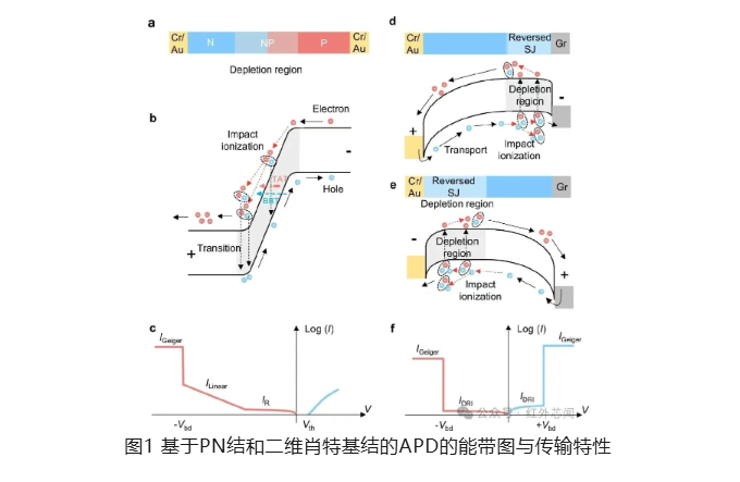
APDs are typically based on PN junctions (as shown in Figure 1a) or Schottky junctions (SJ, as shown in Figures 1d and 1e), utilizing the strong electric field (ε field) of the junction under reverse bias to trigger carrier impact ionization and multiplication. Figure 1 shows the energy band diagrams and transport characteristics of APDs based on PN junctions and 2D Schottky junctions.
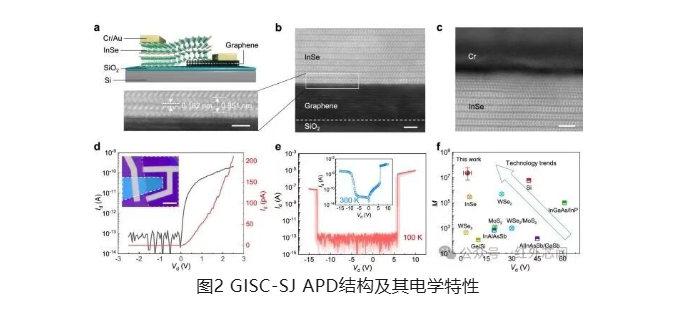
The research team achieved efficient carrier multiplication at low breakdown voltage by constructing an asymmetric Schottky junction. Figure 2a shows a schematic diagram of the GISC-SJ APD structure based on asymmetric graphene/InSe and Cr/InSe junctions. The team characterized the structure and electrical properties of this GISC-SJ APD, with results shown in Figure 2. Experimental results indicate that the device achieves extremely high gain at low breakdown voltage and exhibits bilateral Geiger mode avalanche phenomena.
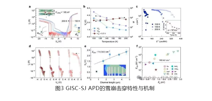
To study the avalanche breakdown characteristics of the GISC-SJ APD, temperature-dependent experiments were conducted, with related results shown in Figure 3. The experiments demonstrate that the device exhibits typical avalanche breakdown behavior at low temperatures and can operate stably at room temperature; the device also has a positive temperature coefficient of ionization rate and an extremely low critical electric field, indicating better carrier multiplication capability at high temperatures.
Based on the excellent electrical performance of the GISC-SJ APD device, researchers thoroughly investigated its detection performance at room temperature, with related results shown in Figure 4. The results show that the device exhibits low dark current and low noise equivalent power at room temperature and can detect extremely low-intensity optical signals.
In summary, this study achieved APD performance with low breakdown voltage and high gain by designing and fabricating an asymmetric Schottky junction (Graphene/InSe/Cr) APD. The device exhibits low dark current and low noise equivalent power at room temperature and can detect extremely low-intensity optical signals. This 2D material-based APD design provides new ideas and methods for developing the next generation of low-power, high-gain photodetectors.
LATEST NEWS
Thank you for visiting the official website of Chongfan Technology. If you have cooperation intentions or suggestions, please contact us through the following methods, and we will reply as soon as possible, thank you!
Address: Room 403, Building 6, Phase III of R&D, No. 36 Xiyong Avenue, High tech Zone, Chongqing, China.
Telephone: +86-13658337211
E-mail: Sales@cfkeji.net
Website: www.cfkeji.net
Mobile Version