Chongfan Technology
News
20
2025
-
07
Sony develops a new three-layer stacked CMOS image sensor, promising significant improvements in various performance aspects.
Author:
According to MEMS Consulting, Sony's Imaging and Sensing Solutions (I&SS) division recently held an investor meeting. During the keynote speech, Sony detailed a promising three-layer stacked CMOS image sensor (CIS) expected to significantly improve performance.
As part of its long-term goals, Sony is heavily investing in new CMOS image sensor technologies, including improved multi-layer stacked CMOS image sensors. Sony has already used stacked CMOS image sensors in several cameras for flagship smartphones, but these sensors are dual-layered: one layer is the photodiode layer, containing the pixel array for light sensing; the other is the logic circuit layer below, responsible for image processing tasks.
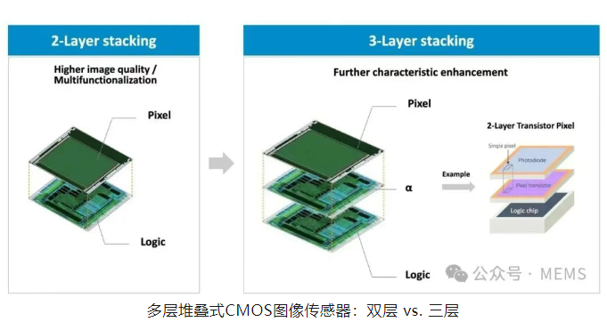
Sony has long been committed to adding a third layer to its stacked CMOS image sensors, essentially meaning expanding image processing capabilities and enhancing image quality. All else being equal, more processing power at the sensor level is generally better.
Enhanced sensor-level processing can improve dynamic range, sensitivity, noise, efficiency, read speed, and resolution. The last advantage is more apparent in video performance than still images. Adding a new sensor layer doesn't change the resolution itself, but by increasing the sensor's speed and performance, it unlocks new video recording modes. Currently, the video resolution of high-resolution CMOS image sensors is often limited by processing bottlenecks; therefore, overcoming this bottleneck can further enhance video performance.
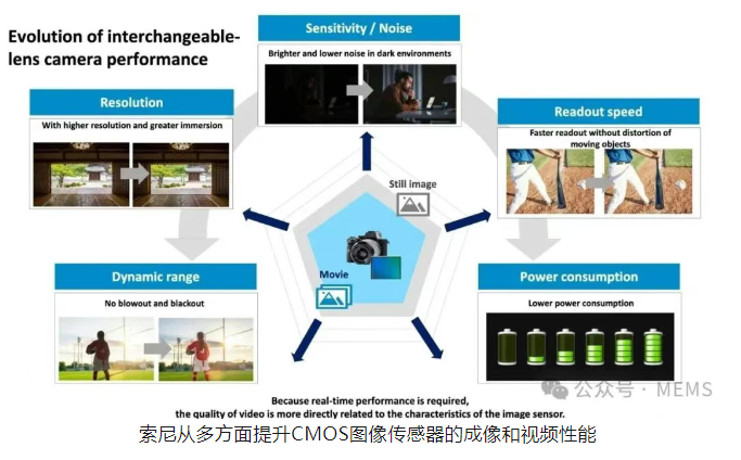
Faster readout speed is crucial for almost every aspect of camera performance, including rolling shutter, burst shooting speed, and autofocus performance.
Improvements in dynamic range are more complex. Better sensor-level image processing can improve dynamic range, but the actual dynamic range of a CMOS image sensor depends on many factors, including the full well capacity of the sensor pixels and the sensor's noise performance. While image processing optimizes noise, full well capacity is a physical state of the actual pixel; adding more layers to the sensor actually reduces full well capacity by physically shrinking the pixels.
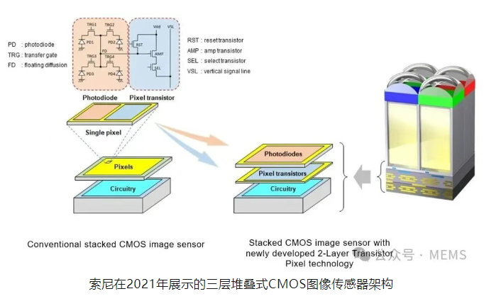
However, Sony explained this situation when it first introduced the concept of a three-layer stacked CMOS image sensor in 2021. As Sony previously demonstrated, the added third layer can also be a pixel transistor layer below the photodiode layer, rather than a second pure processing layer.
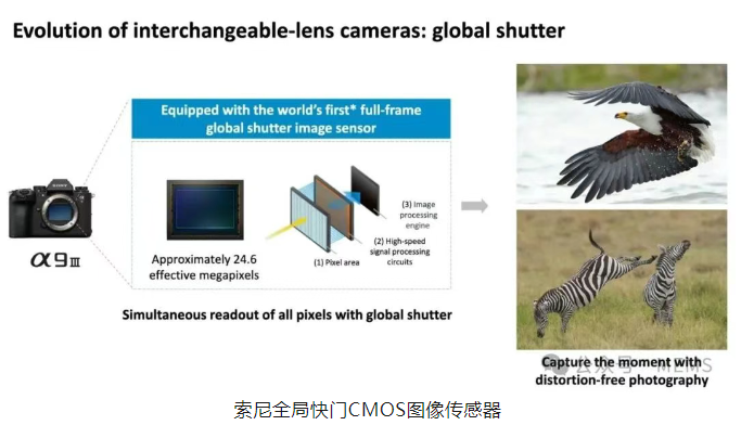
When a three-layer stacked CMOS image sensor will be used in Sony's consumer products remains unknown, but Sony has repeatedly proven its ability to produce groundbreaking CMOS image sensors, such as the global shutter CMOS image sensor used in the Sony full-frame mirrorless camera a9 III (A9M3), and the fast, high-resolution stacked CMOS image sensor in the a1 series cameras. Sony remains committed to the development of full-frame CMOS image sensors, with a bright future ahead.
LATEST NEWS
Thank you for visiting the official website of Chongfan Technology. If you have cooperation intentions or suggestions, please contact us through the following methods, and we will reply as soon as possible, thank you!
Address: Room 403, Building 6, Phase III of R&D, No. 36 Xiyong Avenue, High tech Zone, Chongqing, China.
Telephone: +86-13658337211
E-mail: Sales@cfkeji.net
Website: www.cfkeji.net
Mobile Version