Chongfan Technology
News
12
2025
-
07
Hyperspectral channel density on-chip diffractive speckle spectrometer
Author:
With the advancement of spectral sensors towards portability and intelligence, traditional desktop spectrometers are limited by the trade-off between size and performance, making it difficult to meet the urgent needs of medical, agricultural, and consumer electronics fields for high-resolution, high-bandwidth, and miniaturized devices. In contrast, chip-scale micro-spectrometers have significant advantages in size, weight, and power consumption, providing feasible solutions for on-site rapid detection and embedded spectral sensing. Recently, Professor Xu Ke and Professor Song Qinghai's team at Harbin Institute of Technology (Shenzhen) proposed a silicon-based chip speckle spectrometer based on cascaded disordered metasurfaces. Based on high-transmittance subwavelength phase modulation units, speckle rich in spectral fingerprint information is generated, ultimately achieving high-resolution and wide-bandwidth spectral reconstruction within a sub-square millimeter chip size.
Research Background
Traditional desktop spectrometers rely on complex discrete optical components and precise mechanical structures, making miniaturization and lightweight integration difficult. Chip-level micro-spectrometers, however, have advantages such as small size, light weight, and low power consumption, making them more suitable for the development trend of mobile and portable spectral detection technology. Among them, silicon-based photonic integration technology, due to its high reliability and compatibility with microelectronic processes, has become an ideal carrier for realizing high-performance on-chip spectrometers. However, how to use a small chip size to achieve high spectral resolution and wide spectral range spectral reconstruction simultaneously is a key challenge facing current chip-level spectrometers. Existing on-chip spectrometer technologies (such as dispersive elements, filter arrays, or Fourier transform structures) often have limitations in optical path difference and the number of devices when balancing high resolution and high bandwidth, resulting in problems such as large chip physical size, low data acquisition efficiency, and increased power consumption.
Research Content
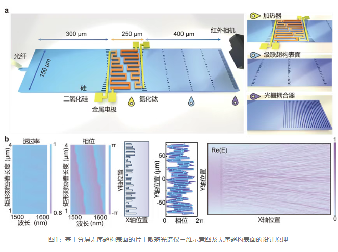
The spectrometer proposed in this study is designed based on the silicon-on-insulator (SOI) platform. The core architecture includes an input single-mode waveguide, a wavefront collimating meta-lens, a cascaded multilayer disordered metasurface, and a multi-mode output diffraction grating ( Figure 1a ). After the single-mode waveguide output mode field is wavefront shaped by the meta-lens, a collimated beam is formed and incident on the cascaded metasurface. The metasurface is composed of subwavelength units of fully etched rectangular grooves. By precisely controlling the length of the grooves, a phase shift of 0 to 2π can be introduced while maintaining high transmittance ( Figure 1b ). According to the Huygens-Fresnel principle, the disordered wavefront generated by the randomly arranged groove array can be converted into the intensity distribution of the waveguide cross-section through interference and diffraction effects, thereby encoding the spectral information into the speckle pattern. Finally, the spectral speckle is output by grating diffraction.
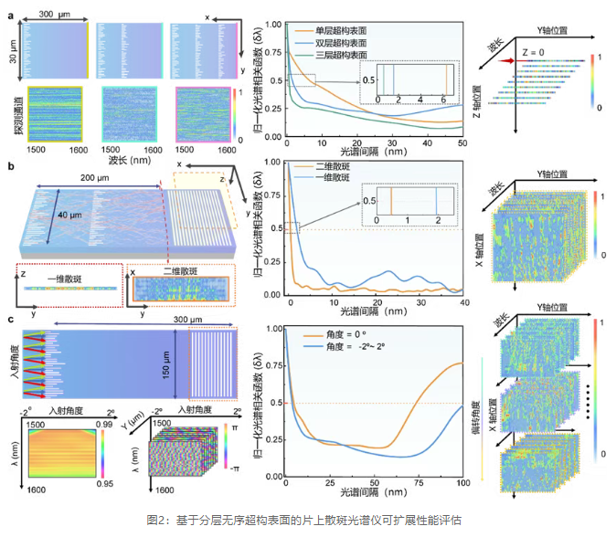
This device improves the number of spectral channels within a small size through three key technologies. First, by introducing multi-level phase modulation units through layered cascaded metasurfaces ( Figure 2a ), the spectral feature density of the output speckle field distribution is significantly increased. Second, a multi-mode diffraction grating is used to achieve waveguide-free space speckle sampling ( Figure 2b ), mapping the one-dimensional intensity distribution to a two-dimensional speckle. Compared with the traditional waveguide array sampling method, this scheme greatly maintains the spatial difference information of the speckle. Finally, by integrating an on-chip thermo-optic modulator ( Figure 2c ), dynamic modulation using the thermo-optic effect is achieved to control the incident angle, expanding the spectral channel capacity in the angle dimension.
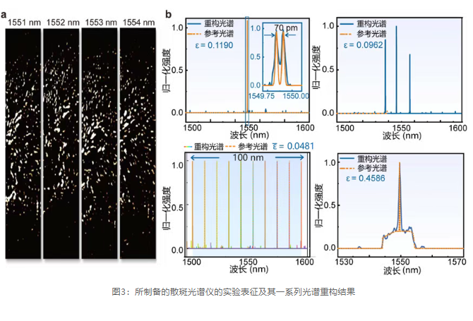
Before spectral reconstruction, the device needs to be pre-calibrated: scan and record the speckle pattern within the working spectral range ( Figure 3a ), and build a spectral-spatial data mapping model based on compressed sensing algorithm. To evaluate the universality of the spectrometer, the experiment selected single-peak, multi-peak composite spectra, and single-peak spectra with Gaussian background superposition as the test sample set. And the relative error analysis is carried out by comparing the measurement results of the commercial spectral analyzer ( Figure 3b ). It can be seen that whether it is a simple single-peak spectrum or a complex mixed spectrum, the prepared spectrometer can achieve high-precision reconstruction, proving the device's general spectral measurement capability and high accuracy.
Future Prospects
Driven by the demand for high-performance miniature spectrometers, research on chip-scale spectrometers is continuously breaking through in the direction of high integration, high resolution, and high bandwidth. This work proposes a silicon-based on-chip spectrometer based on cascaded disordered metasurfaces. Through various on-chip wavefront control mechanisms, high-spectral speckle is generated, and the number of spectral channels is expanded with a compact chip size, thus achieving extremely high on-chip spectral channel density, providing an effective means for achieving high-resolution, high-bandwidth spectral detection. The device is fabricated using standard silicon photonics processes, combining process robustness and mass production potential. In addition, this structure also has the potential to expand the bandwidth across material systems, and is expected to be applied in different application scenarios.
LATEST NEWS
Thank you for visiting the official website of Chongfan Technology. If you have cooperation intentions or suggestions, please contact us through the following methods, and we will reply as soon as possible, thank you!
Address: Room 403, Building 6, Phase III of R&D, No. 36 Xiyong Avenue, High tech Zone, Chongqing, China.
Telephone: +86-13658337211
E-mail: Sales@cfkeji.net
Website: www.cfkeji.net
Mobile Version