09
2025
-
01
Design and Development of Full-Spectrum Photodetectors
Author:
Research on constructing heterojunction strategies to utilize the synergistic effect of materials responsive to different wavelengths to broaden the detection range, suppress device dark current, and improve detection sensitivity has been widely reported. However, the aforementioned research mainly aims to broaden the infrared response of PDs, lacking theoretical and systematic in-depth exploration in aspects such as the interaction at the interface after constructing the heterojunction, charge transport relationships, device mechanical performance and stability, and the impact of heterojunction layer thickness on device performance. In addition, strategies that utilize fluorescent conversion materials to absorb deep ultraviolet-ultraviolet light and emit visible or infrared photons consistent with the PDs response wavelength, thereby enhancing the device's ultraviolet detection performance, have received considerable attention.
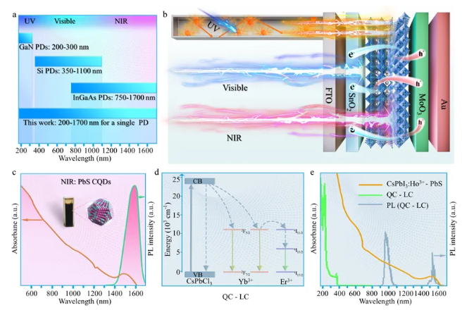
3,By doping rare earth ions (Ce3+, Yb3+, Er3+) into CsPbCI3:Cr3+PQDs to achieve efficient near-infrared (900-1700 nm) quantum cutting emission, with a fluorescence quantum efficiency of 179%. Further, constructing it as a fluorescent concentrator (LC) applied to the outer layer of the device achieves high-performance ultraviolet wavelength response (200-400 nm). Ultimately, the prepared PDs achieved full-spectrum response from 200-1700 nm, while their overall device detection performance exceeded 1012Jones, and exhibited good operational stability.
Research Highlights
a) Firstly, doping Ho3+into CsPbIPQDs, through the study of the optoelectronic properties of the material, it can be concluded that Ho3doping improves the3+luminescence quantum efficiency of PQDs (>>93.5%) and radiative transition rate, reduces its own lattice defects, and achieves efficient electron transport characteristics. At the same time, the ultraviolet light irradiation and thermal stability of the PQDs material have also been greatly improved.PQDs, through the study of the optoelectronic properties of the material, it can be concluded that Ho3b) The combination of PbS quantum dots withPQDs, through the study of the optoelectronic properties of the material, it can be concluded that Ho3PQDs achieved broadband light absorption from visible light to near-infrared II region (400-1700 nm); at the same time, the luminescence intensity decreased after the combination, proving that effective charge transfer was achieved between the two; further, through first-principles calculations, the accuracy of the experimental results was theoretically verified.
c) The preparation of CsPbClPQDs, through the study of the optoelectronic properties of the material, it can be concluded that Ho3:Cr
Jones, and 2.23×10¹²Jones. At the same time, the device has high stability and cycling characteristics.1013Figure 1. (a) Response wavelength range of different types of detectors. (b) Schematic diagram of device structure. (c) Absorption and emission spectra of PbS quantum dots. (d) Energy transfer schematic of CsPbCl1012PQDs. (e) CsPbCl

Previous
Previous
LATEST NEWS
2025-01-09
Design and Development of Full-Spectrum Photodetectors
In recent years, the booming optoelectronic industry has changed the world and extended into many aspects of life. Among them, photodetectors (PDs) with a wide response bandwidth from deep ultraviolet to visible to near-infrared serve as important optoelectronic components and play a key role in daily life.
2025-01-08
Black arsenene multi-spectral integrated field-effect transistors, aiding high-resolution imaging and enhanced secure communication.
With the development of modern communication technology, the demand for broadband, room-temperature infrared, and terahertz (THz) detectors has rapidly increased. These detectors play a crucial role in fields such as telecommunications, security inspection, non-destructive testing, and medical diagnostics. However, existing optical detectors face challenges such as high intrinsic dark current and the need for low-temperature cooling, which limit their efficiency in detecting low-energy photons. Particularly in the terahertz band, the photon energy is insufficient to excite electron transitions from the valence band maximum (VBM) to the conduction band minimum (CBM), making effective optoelectronic conversion difficult. Therefore, researchers have been seeking ultra-broadband detectors that can operate at room temperature and respond to wavelengths ranging from visible light to the terahertz band.
2024-12-30
Laser-based tiered neurons achieve high-speed reservoir computing.
Neuromorphic computing is a computational paradigm that simulates the functions and architecture of biological neurons. A single biological neuron is a powerful computational unit with information processing capabilities, information transmission abilities, and memory functions. Therefore, it is crucial to design a photonic neuromorphic processor that can truly emulate the powerful computational functions of biological neurons.
2025-01-01
Design and Development of Full-Spectrum Photodetectors
In recent years, the rapidly growing optoelectronic industry has changed the world and extended into many aspects of life. Among them, photodetectors (PDs) with a wide spectral response from deep ultraviolet to visible to near-infrared serve as important optoelectronic components and play a key role in daily life.
2024-12-31
High-sensitivity quantum dot photodetectors from deep ultraviolet to near-infrared
In recent years, the rapidly growing optoelectronic industry has changed the world and extended into many aspects of life. Among them, photodetectors (PD) with deep ultraviolet-visible-near infrared full spectrum detection response serve as important optoelectronic components, playing a key role in daily life.

