
Chongfan Technology
News
01
2025
-
01
Design and Development of Full-Spectrum Photodetectors
Author:
Research on constructing heterojunction strategies to utilize the synergistic effect of materials responsive to different wavelengths to broaden the detection range, suppress device dark current, and improve detection sensitivity has been widely reported. However, the aforementioned research mainly aims to broaden the infrared response of PDs, lacking theoretical and systematic in-depth exploration in aspects such as the interaction at the interface after constructing the heterojunction, charge transport relationships, device mechanical performance and stability, and the impact of heterojunction layer thickness on device performance. In addition, strategies that utilize fluorescent conversion materials to absorb deep ultraviolet-ultraviolet light and emit visible or infrared photons consistent with the PDs' response wavelength, thereby enhancing the device's ultraviolet detection performance, have received considerable attention.
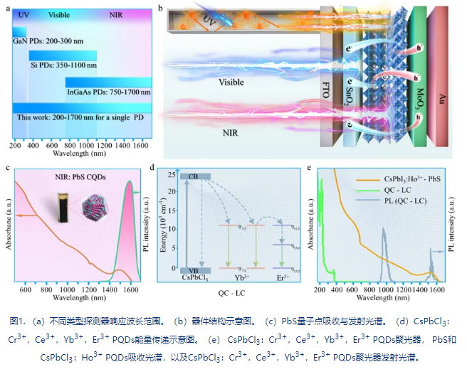
3,By doping rare earth ions (Ce3+, Yb3+, Er3+) into CsPbCl3:Cr3+PQDs, achieving efficient near-infrared (900-1700 nm) quantum cutting emission with a fluorescence quantum efficiency of 179%. Further, constructing it as a fluorescent concentrator (LC) applied to the outer layer of the device achieves high-performance ultraviolet wavelength response (200-400 nm). Ultimately, the prepared PDs achieved full-spectrum response from 200-1700 nm, while the overall device detection performance exceeded 1012Jones, and exhibited good operational stability.
Research Highlights
a) Firstly, by doping Ho3+into CsPbIPQDs, through the study of the optoelectronic performance of the material, it can be concluded that Ho3doping improves the3+PQDs' luminous quantum efficiency (>>93.5%) and radiative transition rate, reducing its own lattice defects, and obtaining efficient electron transport characteristics. At the same time, the ultraviolet light irradiation and thermal stability of thePQDs, through the study of the optoelectronic performance of the material, it can be concluded that Ho3PQDs material have also been greatly improved.PQDs, through the study of the optoelectronic performance of the material, it can be concluded that Ho3b) By combining PbS quantum dots with
PQDs, broadband light absorption from visible light to near-infrared II region (400-1700 nm) was achieved; at the same time, the luminescence intensity decreased after the combination, proving that effective charge transfer was realized between the two; further, through first-principles calculations, the accuracy of the experimental results was theoretically verified.PQDs, through the study of the optoelectronic performance of the material, it can be concluded that Ho3c) The preparation of CsPbCl
d) The combination of the three achieved high sensitivity detection from 200-1700 nm, with detection responses at wavelengths of 260 nm, 460 nm, and 1550 nm reaching 3.19×10¹²Jones, 1.05×10¹³Jones, and 2.23×10¹²Jones, respectively. At the same time, the device exhibits high stability and cyclic usage characteristics.
LATEST NEWS
Thank you for visiting the official website of Chongfan Technology. If you have cooperation intentions or suggestions, please contact us through the following methods, and we will reply as soon as possible, thank you!
Address: Room 403, Building 6, Phase III of R&D, No. 36 Xiyong Avenue, High tech Zone, Chongqing, China.
Telephone: +86-13658337211
E-mail: Sales@cfkeji.net
Website: www.cfkeji.net
Mobile Version