10
2024
-
12
A general optoelectronic imaging platform based on two-dimensional semiconductor wafer-level integration, aiding in near-infrared night vision imaging and short-wave infrared material recognition.
Author:
Photodetectors (PD) are crucial in modern society as they can detect various light-based signals. With the exponential growth in the development of photodetectors, various materials have been tried for manufacturing photodetectors that play a key role in achieving various applications and technologies. However, the lack of a universal system that can integrate all types of photodetectors with silicon-based readout integrated circuits (ROIC) has severely hindered the development of image sensor technology.
According to MEMS Consulting, a research team composed of Fudan University, Shaoxin Laboratory, Shanghai Institute of Technical Physics of the Chinese Academy of Sciences, and Soochow University has recently developed a wafer-scale integrated universal photoelectronic imaging platform based on two-dimensional semiconductor materials, achieving a high-performance, multifunctional, and large-scale integrated imaging system. The related research results were published under the title 'A universal photoelectronic imaging platform with wafer-scale integration of two-dimensional semiconductors' inChipjournal.
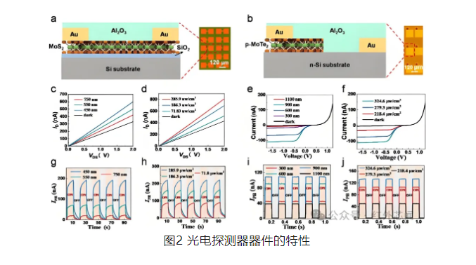
This research focuses on developing a wafer-scale integrated universal photoelectronic imaging platform based on two-dimensional semiconductor materials. The research team employed various innovative methods to achieve this goal. First, the researchers selected multiple two-dimensional materials, including MoS₂, MoTe₂, etc., which have unique photoelectric properties. To facilitate the efficient integration of two-dimensional materials with traditional silicon-based electronic devices, the researchers innovatively developed wafer-scale integration preparation technology. This technology breaks through traditional boundaries, allowing for the precise growth of large-area and high-quality two-dimensional material films directly on a carefully designed substrate, achieving seamless and highly compatible integration between the two, opening new pathways for enhancing the performance of electronic devices.

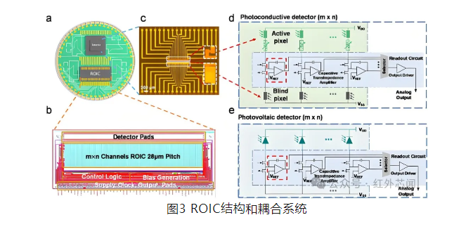
During the device manufacturing process, the research team also optimized the design of the readout circuit (CMOS) to ensure it matched the characteristics of the two-dimensional material detectors. The researchers used advanced micro-nano fabrication technology to create electrodes and interconnection structures, ensuring high performance and reliability of the devices. In addition, the researchers developed special packaging technology to protect the sensitive two-dimensional materials from environmental factors, thereby extending the lifespan of the devices.

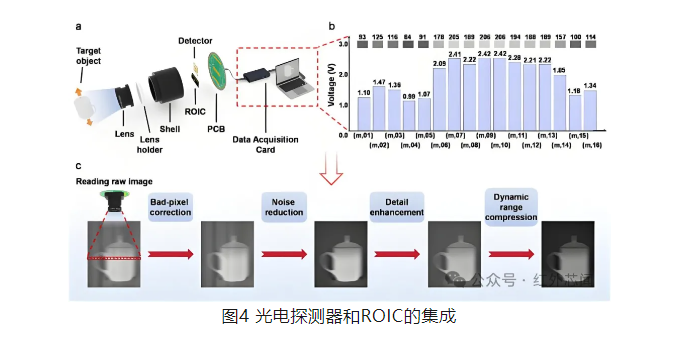
The research team successfully manufactured a large-scale integrated array of two-dimensional semiconductor photodetectors, achieving high resolution and a high frame rate imaging of over 100 frames per second. This system can not only perform conventional visible light imaging but also operate in the near-infrared and short-wave infrared bands, demonstrating excellent multispectral imaging capabilities. Notably, the researchers achieved high-quality color imaging, near-infrared night vision imaging, and short-wave infrared material recognition imaging through a carefully designed optical system and signal processing algorithms.

The research team conducted an in-depth analysis of the advantages and potential applications of this new imaging platform. Compared to traditional silicon-based image sensors, this platform based on two-dimensional materials has a broader spectral response range and can achieve multi-band imaging on a single chip. This feature has significant applications in many fields, such as obtaining information from both surface and deep tissues in medical imaging and identifying different gases and pollutants in environmental monitoring.

Furthermore, the researchers explored the scalability and industrialization prospects of this technology. Although the current manufacturing costs are high, costs are expected to decrease significantly with advancements in two-dimensional material production technology and the realization of scale effects. The research team also proposed several improvement directions, including further enhancing material quality, optimizing device structures, and developing more advanced signal processing algorithms to further improve system performance.
Finally, the researchers looked forward to the future development of this technology. With the continuous progress in two-dimensional material science and engineering, this universal photoelectronic imaging platform is expected to find applications in more fields, such as autonomous driving, augmented reality, and industrial inspection. This research not only promotes the application of two-dimensional materials in the field of optoelectronics but also points the way for the development of the next generation of multifunctional, high-performance imaging systems.
LATEST NEWS
2025-01-09
Design and Development of Full-Spectrum Photodetectors
In recent years, the booming optoelectronic industry has changed the world and extended into many aspects of life. Among them, photodetectors (PDs) with a wide response bandwidth from deep ultraviolet to visible to near-infrared serve as important optoelectronic components and play a key role in daily life.
2025-01-08
Black arsenene multi-spectral integrated field-effect transistors, aiding high-resolution imaging and enhanced secure communication.
With the development of modern communication technology, the demand for broadband, room-temperature infrared, and terahertz (THz) detectors has rapidly increased. These detectors play a crucial role in fields such as telecommunications, security inspection, non-destructive testing, and medical diagnostics. However, existing optical detectors face challenges such as high intrinsic dark current and the need for low-temperature cooling, which limit their efficiency in detecting low-energy photons. Particularly in the terahertz band, the photon energy is insufficient to excite electron transitions from the valence band maximum (VBM) to the conduction band minimum (CBM), making effective optoelectronic conversion difficult. Therefore, researchers have been seeking ultra-broadband detectors that can operate at room temperature and respond to wavelengths ranging from visible light to the terahertz band.
2024-12-30
Laser-based tiered neurons achieve high-speed reservoir computing.
Neuromorphic computing is a computational paradigm that simulates the functions and architecture of biological neurons. A single biological neuron is a powerful computational unit with information processing capabilities, information transmission abilities, and memory functions. Therefore, it is crucial to design a photonic neuromorphic processor that can truly emulate the powerful computational functions of biological neurons.
2025-01-01
Design and Development of Full-Spectrum Photodetectors
In recent years, the rapidly growing optoelectronic industry has changed the world and extended into many aspects of life. Among them, photodetectors (PDs) with a wide spectral response from deep ultraviolet to visible to near-infrared serve as important optoelectronic components and play a key role in daily life.
2024-12-31
High-sensitivity quantum dot photodetectors from deep ultraviolet to near-infrared
In recent years, the rapidly growing optoelectronic industry has changed the world and extended into many aspects of life. Among them, photodetectors (PD) with deep ultraviolet-visible-near infrared full spectrum detection response serve as important optoelectronic components, playing a key role in daily life.

