11
2024
-
11
Novel on-chip integrated waveguide antimonide semiconductor mid-infrared laser
Author:
On-Chip Integration of a Novel Sawtooth Waveguide Structure Antimonide Semiconductor Laser
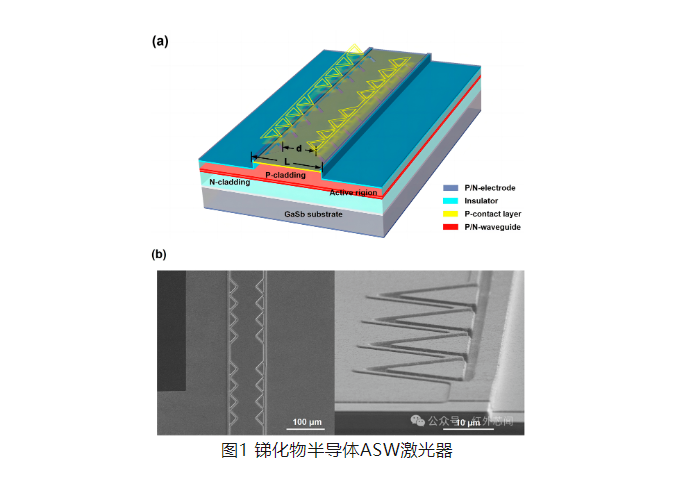
The structure of the antimonide semiconductor ASW laser is shown in Figure 1. The structure design is based on the near-field distribution characteristics of the wide-area waveguide, using two-dimensional time domain finite differential (FDTD) simulation, and setting a series of sawtooth structures along the cavity length direction accurately improves the loss of high-order modes, and also improves the carrier accumulation on both sides of the waveguide.

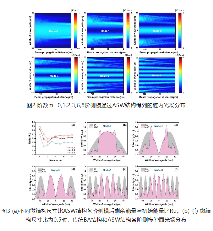
The intracavity optical field distribution of the antimonide semiconductor ASW laser is shown in Figure 2. The sawtooth structure on both sides hardly affects the fundamental mode, and the scattering of higher-order modes increases significantly. The optical field distribution of each order mode of the laser in the cavity surface is shown in fig. 3: its microstructure size ratio (L-d)/L is 0.5, and the residual energy of the fundamental mode is about 1.4 times that of the high order mode. it can be seen that most of the energy of the fundamental mode is retained, while the intensity distribution of the high order mode is significantly reduced on both sides of the waveguide, while the carrier profile and the mode profile of the device are more matched.

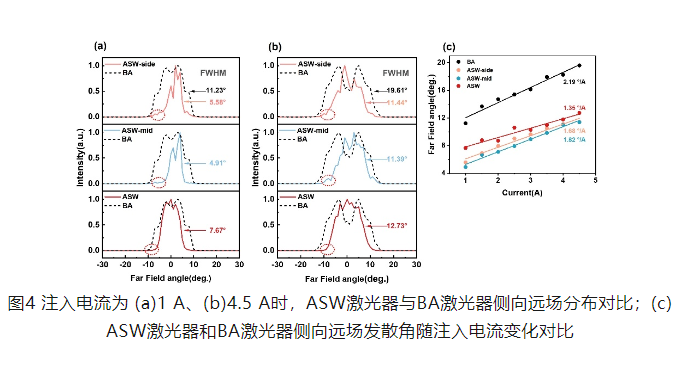
In this study, ASW and BA lasers with the same output aperture are compared. ASW has higher photoelectric efficiency under the equivalent output power of 1.1W. The lateral far-field distribution of the two devices and the relationship between the lateral far-field divergence angle and the injection current are shown in Figure 4: Obviously, the traditional BA laser is a typical multi-lobe far-field, while the ASW laser far-field distribution is more concentrated. In the whole dynamic current range, in addition to the smaller lateral divergence, the dependence of the lateral divergence on the current is reduced from 2.19 °/A to 1.35 °/A, revealing a more stable mode regulation.

Summary and Prospect
LATEST NEWS
2024-10-05
Calculation of the diffracted light field: Regarding Fresnel near-field diffraction, how should the field distribution be calculated after a plane wave encounters a metasurface and experiences a phase jump?
Previously, a friend wanted to see the source code for the article 'Matlab Optical Fresnel Diffraction, Dynamic Visualization of Matlab Curves and Graphics', and the source code is included in this article.
2024-11-15
Academician Chang Ruihua's team has made new progress in short-distance optical communication high-speed interconnection technology.
850nm wavelength multimode vertical-cavity surface-emitting lasers (VCSELs) and multimode fibers (MMFs) have become the ideal choice for short-distance optical interconnects in data centers and supercomputing systems due to their low power consumption and cost-effectiveness.
2024-11-18
Wide spectrum heterojunction self-powered photodetector with linear and circular polarization detection capabilities
Two-dimensional (2D) materials have become a hot research topic due to their unique mechanical, optical and physical properties such as broadband response range, layer-dependent band gap, tunable electronic and optical properties, and high carrier mobility.
2024-11-07
Spin-based Schrodinger Cat States Prepared by Laser Cold Atom Method
The spin-based Schrodinger cat state is prepared by laser cold atom method, and its lifetime reaches the order of minutes, which helps to improve the measurement sensitivity of spin precession phase.

