Chongfan Technology
News
10
2025
-
06
Research progress on the high quantum efficiency mechanism of type-II superlattice infrared detectors
Author:
T2SL Material Characteristics
T2SL is a multilayer film structure in which two different materials are alternately grown in thin layers ranging from several nanometers to tens of nanometers, maintaining strict periodicity. In fact, it is a specific form of layered fine composite material. Due to its advantages such as flexible band gap tunability, high large-area uniformity, high reproducibility and operability, low Auger recombination, and wide spectral response range (3 μm~30 μm), however, the Shockley-Read-Hall (SRH) recombination in T2SL materials limits the diffusion length of photogenerated carriers, resulting in a relatively short carrier lifetime for T2SL. Furthermore, it is difficult to grow thicker, high-quality T2SL epitaxial materials using current processes. Thin epitaxial materials result in insufficient light absorption, hindering the improvement of QE.
Research Progress on High-QE T2SL Infrared Detectors
1. Band Structure Design - Research Progress on High-QE with Increased Absorption Coefficient
In T2SL, the wave function overlap (WFO) is weakened. This change in band alignment can negatively affect the photoelectric conversion process, showing a trend where increasing WFO also increases QE. In 2022, WU et al. from Fudan University proposed a dual strategy to enhance WFO in InAs/AlSb T2SL by adjusting the growth temperature and inserting a blocking layer in the AlSb layer. In the same year, researchers from the Institute of Semiconductors, Chinese Academy of Sciences, reported a high-performance InAs/InAsSb/AlAsSb infrared P-I-N photodetector, as shown in Figure 1. By reducing the thickness of the InAs, InAsSb, and AlAsSb layers and designing a thinner top contact layer to reduce absorption in the contact area, the QE of the device was improved.

Research Progress on Improving QE Using a Thick Absorption Region
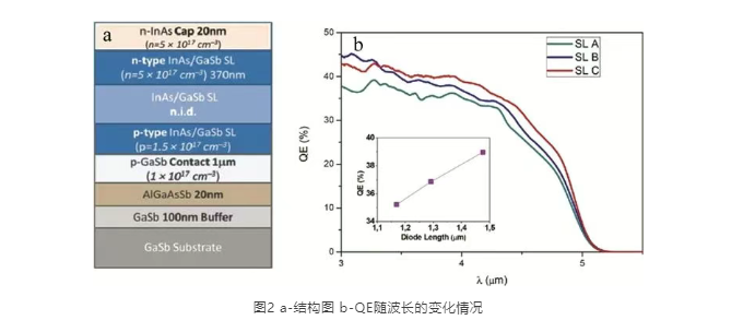
In 2007, NGUYEN et al. from Northwestern University, USA, adjusted the thickness of the absorption layer in a long-wave InAs/GaSb T2SL infrared detector. Increasing the absorption layer thickness from 1 μm to 6 μm increased the device QE from 27% to 54%. In 2013, the mid-wave infrared heterojunction T2SL barrier focal plane detector designed by IRnova in Sweden used a 4 μm thick absorption layer barrier structure, achieving a high QE of 65% at a 50% cutoff wavelength of 5 μm. In 2021, Akdeniz University in Turkey studied the QE of different regions of a device using an N-on-P structure InAs/GaSb T2SL, analyzing the QE components of three T2SL InAs/GaSb infrared photodetectors with the same period length but different I-layer and P-layer thicknesses, as shown in Figure 2. When the layer thickness increased by 0.4 μm, the QE increased from 34% to 40%.
Research Progress on QE of P-type Absorption Region
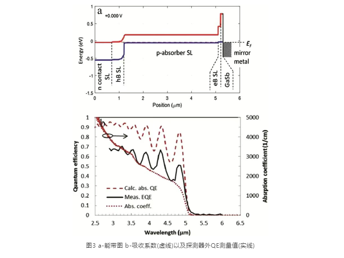
In addition to the above methods, the diffusion length of carriers can be increased by adjusting the P-type doping of the absorption region, thereby increasing the QE. In 2017, ASPLUND et al. from IRnova in Sweden studied the relationship between carrier diffusion length and external QE. The device structure is shown in Figure 3a, using a P-type doped absorption region, ultimately achieving high QE performance. At an operating temperature of 80 K and a wavelength of 3 μm, the measured QE of the device reached 80%, as shown in Figure 3b. In 2020, SOIBEL et al. in the US found that the increase in QE with temperature is due to the increase in the minority carrier (hole) diffusion length, while the increase in QE with bias is due to the increase in depletion width. The results are shown in the figure, where the QE increases from 30% to 60% as the temperature increases from T=50 K to T=180 K.
Research Progress on Improving QE by Improving Materials
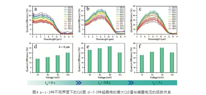
Two common manifestations of carrier localization are extremely long carrier lifetimes and blue shift of the PL peak at low temperatures. By optimizing material quality to reduce defects and SRH centers, the carrier lifetime can be increased, optimizing device QE. In 2017, BI et al. from Fudan University studied the relationship between T2SL residual strain and QE using InAs/GaSb superlattices with three different interface compositions, as shown in Figure 4. The specific scheme is to use an appropriate amount of indium (In) deposition to improve the interface flatness, thereby increasing the carrier lifetime and further increasing the QE of the device. As the In deposition time increases, the peak QE increases from 23% to 50%.
Other Related Research
Optical control is also a relatively direct and effective way to increase QE. Optical control usually uses surface micro-nano structures to control the spatial distribution of incident light, such as using photonic crystals, light trapping structures, and surface plasmon enhancement. Various microfabrication methods and pattern transfer techniques are used to design and fabricate Wiener structures on the surface of the device. The dimensions can be precisely controlled at the nanometer level, thereby increasing the absorption efficiency of infrared light.
Summary
This study summarizes the current methods and research progress for improving the QE of mid-long wave T2SL infrared detectors. The magnitude of the absorption coefficient, the thickness of the absorption layer, the diffusion length, and the length of the carrier lifetime all have a significant impact on QE. This study focuses on the influence mechanism of band structure design, absorption layer thickness setting, absorption layer doping type selection, and material improvement on the QE of T2SL infrared detectors and the progress made to a certain extent. Overall, many research institutions at home and abroad have conducted extensive research on improving the QE of T2SL infrared detectors. Judging from the reported results, there is still a large gap between domestic and foreign research, and improvements in the mechanism are urgently needed. This research has strong guiding significance for the future design of high-QE T2SL infrared detectors.
Previous
Previous
LATEST NEWS
2025-12-17
Beijing Institute of Technology Review: Infrared Detectors for In-Memory Sensing and Computing
2025-12-17
High-performance III-V family infrared detectors
Since the advent of infrared detectors in the 1940s, their technological framework has undergone leapfrog development, with significant expansions in both device types and performance.
Thank you for visiting the official website of Chongfan Technology. If you have cooperation intentions or suggestions, please contact us through the following methods, and we will reply as soon as possible, thank you!
Address: Room 403, Building 6, Phase III of R&D, No. 36 Xiyong Avenue, High tech Zone, Chongqing, China.
Telephone: +86-13658337211
E-mail: Sales@cfkeji.net
Website: www.cfkeji.net
Mobile Version